SLVSES4C September 2019 – June 2021 TPS54J060
PRODUCTION DATA
- 1 Features
- 2 Applications
- 3 Description
- 4 Revision History
- 5 Pin Configuration and Functions
- 6 Specifications
-
7 Detailed Description
- 7.1 Overview
- 7.2 Functional Block Diagram
- 7.3
Feature Description
- 7.3.1 Enable and Internal LDO
- 7.3.2 Split Rail and External LDO
- 7.3.3 Output Voltage Setting
- 7.3.4 Soft Start and Output-Voltage Tracking
- 7.3.5 Frequency and Operation Mode Selection
- 7.3.6 D-CAP3 Control
- 7.3.7 Current Sense and Positive Overcurrent Protection
- 7.3.8 Low-side FET Negative Current Limit
- 7.3.9 Power Good
- 7.3.10 Overvoltage and Undervoltage Protection
- 7.3.11 Out-Of-Bounds Operation (OOB)
- 7.3.12 Output Voltage Discharge
- 7.3.13 UVLO Protection
- 7.3.14 Thermal Shutdown
- 7.4 Device Functional Modes
-
8 Application and Implementation
- 8.1 Application Information
- 8.2
Typical Application
- 8.2.1 Design Requirements
- 8.2.2
Detailed Design Procedure
- 8.2.2.1 Choose the Switching Frequency and Operation Mode (MODE Pin)
- 8.2.2.2 Choose the Output Inductor (L)
- 8.2.2.3 Set the Current Limit (TRIP)
- 8.2.2.4 Choose the Output Capacitors (COUT)
- 8.2.2.5 Choose the Input Capacitors (CIN)
- 8.2.2.6 Feedback Network (FB Pin)
- 8.2.2.7 Soft Start Capacitor (SS/REFIN Pin)
- 8.2.2.8 EN Pin Resistor Divider
- 8.2.2.9 VCC Bypass Capacitor
- 8.2.2.10 BOOT Capacitor
- 8.2.2.11 Series BOOT Resistor and RC Snubber
- 8.2.2.12 PGOOD Pullup Resistor
- 8.2.3 Application Curves
- 9 Power Supply Recommendations
- 10Layout
- 11Device and Documentation Support
- 12Mechanical, Packaging, and Ordering Information
Package Options
Mechanical Data (Package|Pins)
- RPG|14
Thermal pad, mechanical data (Package|Pins)
Orderable Information
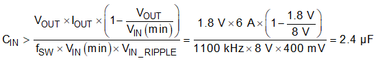
8.2.2.5 Choose the Input Capacitors (CIN)
The TPS54J060 requires input bypass capacitors between the VIN and PGND pins to bypass the power-stage. The bypass capacitors must be placed as close as possible to the pins of the IC as the layout will allow. At least 10 µF of ceramic capacitance and a 0.01-µF to 0.1-µF high frequency ceramic bypass capacitor is required. The high frequency bypass capacitor minimizes high frequency voltage overshoot across the power-stage. The ceramic capacitors must be high-quality dielectric of X5R or X7R for their high capacitance-to-volume ratio and stable characteristics across temperature. In addition to this, more bulk capacitance can be needed on the input depending on the application to minimize variations on the input voltage during transient conditions.
The input capacitance required to meet a specific input ripple target can be calculated with Equation 23. A recommended target input voltage ripple is 5% the minimum input voltage, 400 mV in this example. The calculated input capacitance is 2.4 µF and the minimum input capacitance of 10 µF exceeds this. This example meets these two requirements with two 4.7-µF 0603 25-V ceramic capacitors and two 10-µF 1206 25-V ceramic capacitors.
The capacitor must also have an RMS current rating greater than the maximum input RMS current in the application. The input RMS current the input capacitors must support is calculated by Equation 24 and is 2.5 A in this example. The ceramic input capacitors have a current rating much greater than this.

For applications requiring bulk capacitance on the input, such as ones with low input voltage and high current, the selection process in this article is recommended.