SLVSES4C September 2019 – June 2021 TPS54J060
PRODUCTION DATA
- 1 Features
- 2 Applications
- 3 Description
- 4 Revision History
- 5 Pin Configuration and Functions
- 6 Specifications
-
7 Detailed Description
- 7.1 Overview
- 7.2 Functional Block Diagram
- 7.3
Feature Description
- 7.3.1 Enable and Internal LDO
- 7.3.2 Split Rail and External LDO
- 7.3.3 Output Voltage Setting
- 7.3.4 Soft Start and Output-Voltage Tracking
- 7.3.5 Frequency and Operation Mode Selection
- 7.3.6 D-CAP3 Control
- 7.3.7 Current Sense and Positive Overcurrent Protection
- 7.3.8 Low-side FET Negative Current Limit
- 7.3.9 Power Good
- 7.3.10 Overvoltage and Undervoltage Protection
- 7.3.11 Out-Of-Bounds Operation (OOB)
- 7.3.12 Output Voltage Discharge
- 7.3.13 UVLO Protection
- 7.3.14 Thermal Shutdown
- 7.4 Device Functional Modes
-
8 Application and Implementation
- 8.1 Application Information
- 8.2
Typical Application
- 8.2.1 Design Requirements
- 8.2.2
Detailed Design Procedure
- 8.2.2.1 Choose the Switching Frequency and Operation Mode (MODE Pin)
- 8.2.2.2 Choose the Output Inductor (L)
- 8.2.2.3 Set the Current Limit (TRIP)
- 8.2.2.4 Choose the Output Capacitors (COUT)
- 8.2.2.5 Choose the Input Capacitors (CIN)
- 8.2.2.6 Feedback Network (FB Pin)
- 8.2.2.7 Soft Start Capacitor (SS/REFIN Pin)
- 8.2.2.8 EN Pin Resistor Divider
- 8.2.2.9 VCC Bypass Capacitor
- 8.2.2.10 BOOT Capacitor
- 8.2.2.11 Series BOOT Resistor and RC Snubber
- 8.2.2.12 PGOOD Pullup Resistor
- 8.2.3 Application Curves
- 9 Power Supply Recommendations
- 10Layout
- 11Device and Documentation Support
- 12Mechanical, Packaging, and Ordering Information
Package Options
Mechanical Data (Package|Pins)
- RPG|14
Thermal pad, mechanical data (Package|Pins)
Orderable Information
8.2.2.1 Choose the Switching Frequency and Operation Mode (MODE Pin)
The switching frequency and light load mode of operation are configured by the resistor on the MODE pin. From Table 7-1, the MODE pin is connected to VCC to set a 1100-kHz switching frequency with discontinuous conduction mode and skip mode enabled at light loads.
When selecting the switching frequency of a buck converter, the minimum on-time and minimum off-time must be considered. Equation 6 calculates the maximum fSW before being limited by the minimum on-time. When hitting the minimum on-time limits of a converter with D-CAP3 control, the effective switching frequency will change to keep the output voltage regulated. This calculation ignores resistive drops in the converter to give a worst case estimation.

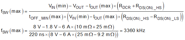
Equation 7 calculates the maximum fSW before being limited by the minimum off-time. When hitting the minimum off-time limits of a converter with D-CAP3 control, the operating duty cycle will max out and the output voltage will begin to drop with the input voltage. This equation requires the DC resistance of the inductor, RDCR, selected in the following step so this preliminary calculation assumes a resistance of 10 mΩ. If you are operating near the maximum fSW limited by the minimum off-time, the variation in resistance across temperature must be considered when using Equation 7. The selected fSW of 1100 kHz is below the two calculated maximum values.