SLVSES4C September 2019 – June 2021 TPS54J060
PRODUCTION DATA
- 1 Features
- 2 Applications
- 3 Description
- 4 Revision History
- 5 Pin Configuration and Functions
- 6 Specifications
-
7 Detailed Description
- 7.1 Overview
- 7.2 Functional Block Diagram
- 7.3
Feature Description
- 7.3.1 Enable and Internal LDO
- 7.3.2 Split Rail and External LDO
- 7.3.3 Output Voltage Setting
- 7.3.4 Soft Start and Output-Voltage Tracking
- 7.3.5 Frequency and Operation Mode Selection
- 7.3.6 D-CAP3 Control
- 7.3.7 Current Sense and Positive Overcurrent Protection
- 7.3.8 Low-side FET Negative Current Limit
- 7.3.9 Power Good
- 7.3.10 Overvoltage and Undervoltage Protection
- 7.3.11 Out-Of-Bounds Operation (OOB)
- 7.3.12 Output Voltage Discharge
- 7.3.13 UVLO Protection
- 7.3.14 Thermal Shutdown
- 7.4 Device Functional Modes
-
8 Application and Implementation
- 8.1 Application Information
- 8.2
Typical Application
- 8.2.1 Design Requirements
- 8.2.2
Detailed Design Procedure
- 8.2.2.1 Choose the Switching Frequency and Operation Mode (MODE Pin)
- 8.2.2.2 Choose the Output Inductor (L)
- 8.2.2.3 Set the Current Limit (TRIP)
- 8.2.2.4 Choose the Output Capacitors (COUT)
- 8.2.2.5 Choose the Input Capacitors (CIN)
- 8.2.2.6 Feedback Network (FB Pin)
- 8.2.2.7 Soft Start Capacitor (SS/REFIN Pin)
- 8.2.2.8 EN Pin Resistor Divider
- 8.2.2.9 VCC Bypass Capacitor
- 8.2.2.10 BOOT Capacitor
- 8.2.2.11 Series BOOT Resistor and RC Snubber
- 8.2.2.12 PGOOD Pullup Resistor
- 8.2.3 Application Curves
- 9 Power Supply Recommendations
- 10Layout
- 11Device and Documentation Support
- 12Mechanical, Packaging, and Ordering Information
Package Options
Mechanical Data (Package|Pins)
- RPG|14
Thermal pad, mechanical data (Package|Pins)
Orderable Information
8.2.2.7 Soft Start Capacitor (SS/REFIN Pin)
The capacitor placed on the SS/REFIN pin can be used to extend the soft-start time past the internal 1.5-ms soft start. This example uses a 2-ms soft start time and the required external capacitance can be calculated with Equation 28. In this example, a 22-nF capacitor is used.
Equation 28. 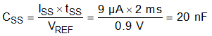
Note: A minimum capacitor value of 1 nF is required at the SS/REFIN pin to help bypass noise.
Also, the SS/REFIN capacitor must use the AGND pin for its ground. Note, any CSS
calculation that uses a soft-start time of less than 1.5 ms will be ignored by the internal
soft-start time circuit. Therefore, selecting a capacitor less than or equal to 15 nF will
result in the internal default 1.5 ms soft-start time.