SLVSFJ0B March 2021 – October 2021 TPS61379-Q1
PRODUCTION DATA
- 1 Features
- 2 Applications
- 3 Description
- 4 Revision History
- 5 Device Comparison Table
- 6 Pin Configuration and Functions
- 7 Specifications
-
8 Detailed Description
- 8.1 Overview
- 8.2 Functional Block Diagrams
- 8.3
Feature Description
- 8.3.1 VCC Power Supply
- 8.3.2 Input Undervoltage Lockout (UVLO)
- 8.3.3 Enable and Soft Start
- 8.3.4 Shut Down
- 8.3.5 Switching Frequency Setting
- 8.3.6 Spread Spectrum Frequency Modulation
- 8.3.7 Bootstrap
- 8.3.8 Load Disconnect
- 8.3.9 MODE/SYNC Configuration
- 8.3.10 Overvoltage Protection (OVP)
- 8.3.11 Output Short Protection/Hiccup
- 8.3.12 Power-Good Indicator
- 8.3.13 Thermal Shutdown
- 8.4 Device Functional Modes
-
9 Application and Implementation
- 9.1 Application Information
- 9.2
Typical Application
- 9.2.1 Design Requirements
- 9.2.2 Detailed Design Procedure
- 9.2.3 Application Curves
- 10Power Supply Recommendations
- 11Layout
- 12Device and Documentation Support
- 13Mechanical, Packaging, and Orderable Information
Package Options
Mechanical Data (Package|Pins)
- RTE|16
Thermal pad, mechanical data (Package|Pins)
- RTE|16
Orderable Information
9.2.2.6.2 Loop Compensation Design Steps
With the small signal models coming out, the next step is to calculate the compensation network parameters with the given inductor and output capacitance.
- Set the Cross Over Frequency, ƒC.
The first step is to set the loop crossover frequency, ƒC. The higher crossover frequency, the faster the loop response is. It is generally accepted that the loop gain cross over no higher than the lower of either 1/10 of the switching frequency, ƒSW, or 1/5 of the RHPZ frequency, ƒRHPZ. Then calculate the loop compensation network values of RC, CC, and CP by the following equations.
- Set the Compensation Resistor, RC.
By placing ƒZ below ƒC, for frequencies above ƒC, RC | | REA ~ = RC and so RC × GEA sets the compensation gain. Setting the compensation gain, KCOMP-dB, at ƒZ, results in the total loop gain, T(s) = KPS(s) × HEA(s) being zero at ƒC.
Therefore, to approximate a single-pole roll-off up to fP2, rearrange Equation 17 to solve for RC so that the compensation gain, KEA, at fC is the negative of the gain, KPS, read at frequency fC for the power stage bode plot or more simply:
Equation 21.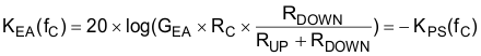
where
- KEA is gain of the error amplifier network
- KPS is the gain of the power stage
- GEA is the transconductance of the amplifier, the typical value of GEA = 70 µA / V
- Set the Compensation Zero capacitor, CC.
Place the compensation zero at the power stage ROUT ,COUT pole’s position to get:
Equation 22.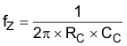
Set ƒZ = ƒP, and get
Equation 23.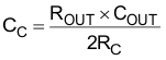
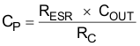
- Set the Compensation Pole Capacitor, CP.
Place the compensation pole at the zero produced by the RESR and the COUT. It is useful for canceling unhelpful effects of the ESR zero.
Equation 24.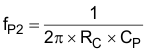 Equation 25.
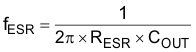
Set ƒP2 = ƒESR, and get
Equation 26.