SLVSFJ0B March 2021 – October 2021 TPS61379-Q1
PRODUCTION DATA
- 1 Features
- 2 Applications
- 3 Description
- 4 Revision History
- 5 Device Comparison Table
- 6 Pin Configuration and Functions
- 7 Specifications
-
8 Detailed Description
- 8.1 Overview
- 8.2 Functional Block Diagrams
- 8.3
Feature Description
- 8.3.1 VCC Power Supply
- 8.3.2 Input Undervoltage Lockout (UVLO)
- 8.3.3 Enable and Soft Start
- 8.3.4 Shut Down
- 8.3.5 Switching Frequency Setting
- 8.3.6 Spread Spectrum Frequency Modulation
- 8.3.7 Bootstrap
- 8.3.8 Load Disconnect
- 8.3.9 MODE/SYNC Configuration
- 8.3.10 Overvoltage Protection (OVP)
- 8.3.11 Output Short Protection/Hiccup
- 8.3.12 Power-Good Indicator
- 8.3.13 Thermal Shutdown
- 8.4 Device Functional Modes
-
9 Application and Implementation
- 9.1 Application Information
- 9.2
Typical Application
- 9.2.1 Design Requirements
- 9.2.2 Detailed Design Procedure
- 9.2.3 Application Curves
- 10Power Supply Recommendations
- 11Layout
- 12Device and Documentation Support
- 13Mechanical, Packaging, and Orderable Information
Package Options
Mechanical Data (Package|Pins)
- RTE|16
Thermal pad, mechanical data (Package|Pins)
- RTE|16
Orderable Information
3 Description
The TPS61379-Q1 is a fully integrated synchronous boost converter with load disconnect function integrated. The input voltage covers 2.3 V to 14 V, while the maximal output voltage is up to 18.5 V. The switching current limit is 2 A typical. It consumes 25-μA quiescent current from VIN.
The TPS61379-Q1 employs the peak current mode control with the switching frequency programmable from 200 kHz to 2.2 MHz. The device works in fixed frequency PWM operation in medium to heavy load. There are two optional modes in light load by configuring the MODE pin: auto PFM mode and forced PWM to balance the efficiency and noise immunity in light load. The switching frequency can be synchronized to an external clock. The TPS61379-Q1 uses the spread spectrum of the internal clock to be more EMI friendly at FPWM mode. In addition, there is an internal soft-start time to limit the inrush current.
The TPS61379-Q1 has various fixed output voltage versions to save the external feedback resistor. It supports the external loop compensation so that the stability and transient response can be optimized at wider VOUT/VIN ranges. It also integrates robust protection features including the output short protection, output overvoltage protection, and thermal shutdown protection. The TPS61379-Q1 is available in a 3-mm × 3-mm 16-pin QFN package with wettable flank.
| PART NUMBER | PACKAGE(1) | BODY SIZE (NOM) |
|---|---|---|
| TPS61379-Q1 | VQFN-16 | 3.0-mm × 3.0-mm |
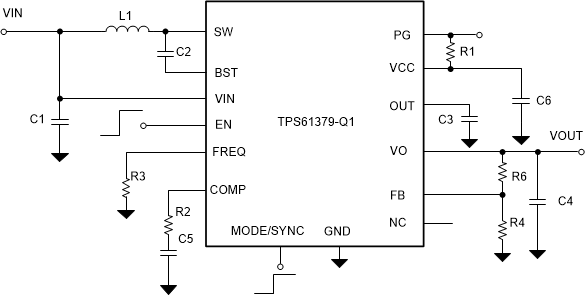
 Typical
Application