SLVSFJ0B March 2021 – October 2021 TPS61379-Q1
PRODUCTION DATA
- 1 Features
- 2 Applications
- 3 Description
- 4 Revision History
- 5 Device Comparison Table
- 6 Pin Configuration and Functions
- 7 Specifications
-
8 Detailed Description
- 8.1 Overview
- 8.2 Functional Block Diagrams
- 8.3
Feature Description
- 8.3.1 VCC Power Supply
- 8.3.2 Input Undervoltage Lockout (UVLO)
- 8.3.3 Enable and Soft Start
- 8.3.4 Shut Down
- 8.3.5 Switching Frequency Setting
- 8.3.6 Spread Spectrum Frequency Modulation
- 8.3.7 Bootstrap
- 8.3.8 Load Disconnect
- 8.3.9 MODE/SYNC Configuration
- 8.3.10 Overvoltage Protection (OVP)
- 8.3.11 Output Short Protection/Hiccup
- 8.3.12 Power-Good Indicator
- 8.3.13 Thermal Shutdown
- 8.4 Device Functional Modes
-
9 Application and Implementation
- 9.1 Application Information
- 9.2
Typical Application
- 9.2.1 Design Requirements
- 9.2.2 Detailed Design Procedure
- 9.2.3 Application Curves
- 10Power Supply Recommendations
- 11Layout
- 12Device and Documentation Support
- 13Mechanical, Packaging, and Orderable Information
Package Options
Mechanical Data (Package|Pins)
- RTE|16
Thermal pad, mechanical data (Package|Pins)
- RTE|16
Orderable Information
9.2.2.6.1 Small Signal Model
The TPS61379-Q1 uses the fixed frequency peak current mode control. There is an internal adaptive slope compensation to avoid the subharmonic oscillation. With the inductor current information sensed, the small-signal model of the power stage reduces from a two-pole system, created by L and COUT, to a single-pole system, created by ROUT and COUT. The single-pole system is easily used with the loop compensation. Figure 9-2 shows the equivalent small signal elements of a boost converter.
The small signal of power stage is:

where
- D is the duty cycle
- ROUT is the output load resistor
- RSENSE is the equivalent internal current sense resistor, which is typically 118 mΩ
The single pole of the power stage is:
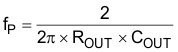
where
- COUT is the output capacitance. For a boost converter having multiple, identical output capacitors in parallel, simply combine the capacitors with the equivalent capacitance
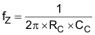
The zero created by the ESR of the output capacitor is:
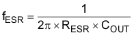
where
- RESR is the equivalent resistance in series of the output capacitor
The right-hand plane zero is:
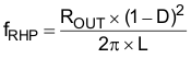
where
- D is the duty cycle
- ROUT is the output load resistor
- L is the inductance
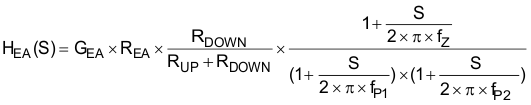
Equation 17 shows the equation for feedback resistor network and the error amplifier.
where
- REA is the output impedance of the error amplifier and typical REA = 500 MΩ.
- ƒP1, ƒP2 is the pole's frequency of the compensation, fZ is the zero’s frequency of the compensation network
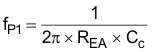
where
- CC is the zero capacitor compensation
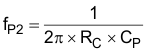
where
- CP is the pole capacitor compensation
- RC is the resistor of the compensation network