SLVSFJ0B March 2021 – October 2021 TPS61379-Q1
PRODUCTION DATA
- 1 Features
- 2 Applications
- 3 Description
- 4 Revision History
- 5 Device Comparison Table
- 6 Pin Configuration and Functions
- 7 Specifications
-
8 Detailed Description
- 8.1 Overview
- 8.2 Functional Block Diagrams
- 8.3
Feature Description
- 8.3.1 VCC Power Supply
- 8.3.2 Input Undervoltage Lockout (UVLO)
- 8.3.3 Enable and Soft Start
- 8.3.4 Shut Down
- 8.3.5 Switching Frequency Setting
- 8.3.6 Spread Spectrum Frequency Modulation
- 8.3.7 Bootstrap
- 8.3.8 Load Disconnect
- 8.3.9 MODE/SYNC Configuration
- 8.3.10 Overvoltage Protection (OVP)
- 8.3.11 Output Short Protection/Hiccup
- 8.3.12 Power-Good Indicator
- 8.3.13 Thermal Shutdown
- 8.4 Device Functional Modes
-
9 Application and Implementation
- 9.1 Application Information
- 9.2
Typical Application
- 9.2.1 Design Requirements
- 9.2.2 Detailed Design Procedure
- 9.2.3 Application Curves
- 10Power Supply Recommendations
- 11Layout
- 12Device and Documentation Support
- 13Mechanical, Packaging, and Orderable Information
Package Options
Mechanical Data (Package|Pins)
- RTE|16
Thermal pad, mechanical data (Package|Pins)
- RTE|16
Orderable Information
9.2.2.3 Selecting the Inductor
A boost converter normally requires two main passive components for storing the energy during the power conversion: an inductor and an output capacitor. The inductor affects the steady state efficiency (including the ripple and efficiency) as well as the transient behavior and loop stability, which makes the inductor the most critical component in application.
When selecting the inductor, as well as the inductance, the other important parameters are:
- The maximum current rating (RMS and peak current must be considered)
- The series resistance
- Operating temperature
The TPS61379-Q1 has built-in slope compensation to avoid subharmonic oscillation associated with the current mode control. If the inductor value is too low and makes the inductor peak-to-peak ripple higher than 2 A, the slope compensation may not be adequate, and the loop can be unstable. Therefore, it is recommended to make the peak-to-peak current ripple between 800 mA to 2 A when selecting the inductor.
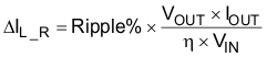
The inductance can be calculated by Equation 3, Equation 4, and Equation 5:
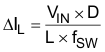
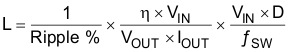
where
- ΔIL is the peak-peak inductor current ripple
- VIN is the input voltage
- D is the duty cycle
- L is the inductor
- ƒSW is the switching frequency
- Ripple % is the ripple ration versus the DC current
- VOUT is the output voltage
- IOUT is the output current
- η is the efficiency
The current flowing through the inductor is the inductor ripple current plus the average input current. During power up, load faults, or transient load conditions, the inductor current can increase above the peak inductor current calculated.
Inductor values can have ±20% or even ±30% tolerance with no current bias. When the inductor current approaches the saturation level, its inductance can decrease 20% to 35% from the value at 0-A bias current depending on how the inductor vendor defines saturation. When selecting an inductor, make sure its rated current, especially the saturation current, is larger than its peak current during the operation.
The inductor peak current varies as a function of the load, the switching frequency, the input and output voltages and it can be calculated by Equation 6 and Equation 7.
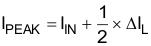
where
- IPEAK is the peak current of the inductor
- IIN is the input average current
- ΔIL is the ripple current of the inductor
The input DC current is determined by the output voltage, the output current can be calculated by:
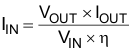
where
- IIN is the input current of the inductor
- VOUT is the output voltage
- VIN is the input voltage
- η is the efficiency
While the inductor ripple current depends on the inductance, the frequency, the input voltage, and duty cycle are calculated by Equation 3. Replace Equation 3 and Equation 7 into Equation 6 and get the inductor peak current:
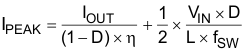
where
- IPEAK is the peak current of the inductor
- IOUT is the output current
- D is the duty cycle
- η is the efficiency
- VIN is the input voltage
- L is the inductor
- ƒSW is the switching frequency
The heat rating current (RMS) is as below:
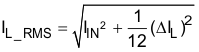
where
- IL_RMS is the RMS current of the inductor
- IIN is the input current of the inductor
- ΔIL is the ripple current of the inductor
It is important that the peak current does not exceed the inductor saturation current and the RMS current is not over the temperature related rating current of the inductors.
For a given physical inductor size, increasing inductance usually results in an inductor with lower saturation current. The total losses of the coil consists of the DC resistance (DCR) loss and the following frequency dependent loss:
- The losses in the core material (magnetic hysteresis loss, especially at high switching frequencies)
- Additional losses in the conductor from the skin effect (current displacement at high frequencies)
- Magnetic field losses of the neighboring windings (proximity effect)
For a certain inductor, the larger current ripple (smaller inductor) generates the higher DC and also the frequency-dependent loss. An inductor with lower DCR is basically recommended for higher efficiency. However, it is usually a tradeoff between the loss and foot print. Table 9-2 lists some recommended inductors.
| PART NUMBER | L (μH) | DCR TYP (mΩ) MAX | SATURATION CURRENT (A) | SIZE (L × W × H mm) | VENDOR(1) |
|---|---|---|---|---|---|
| XGL3515-451ME | 0.45 | 8.2 | 3.2 | 3.5 × 3.2 × 1.5 | Coilcraft |
| XGL3515-102ME | 1 | 18.5 | 2.2 | 3.5 × 3.2 × 1.5 | Coilcraft |
| TFM252012ALMAR47MTAA | 0.47 | 19 | 4.9 | 3.2 × 2.5 × 1.2 | TDK |
| TFM252012ALMA1R0MTAA | 1 | 35 | 4.7 | 3.2 × 2.5 × 1.2 | TDK |