SLVSFM1A March 2021 – November 2023 TPS62902
PRODUCTION DATA
- 1
- 1 Features
- 2 Applications
- 3 Description
- 4 Revision History
- 5 Pin Configuration and Functions
- 6 Specifications
-
7 Detailed Description
- 7.1 Overview
- 7.2 Functional Block Diagram
- 7.3
Feature Description
- 7.3.1 Mode Selection and Device Configuration MODE/S-CONF
- 7.3.2 Adjustable VO Operation (External Voltage Divider)
- 7.3.3 Setable VO Operation (VSET and Internal Voltage Divider)
- 7.3.4 Soft Start / Tracking (SS/TR)
- 7.3.5 Smart Enable with Precise Threshold
- 7.3.6 Power Good (PG)
- 7.3.7 Undervoltage Lockout (UVLO)
- 7.3.8 Current Limit And Short Circuit Protection
- 7.3.9 Thermal Shutdown
- 7.4 Device Functional Modes
-
8 Application and Implementation
- 8.1 Application Information
- 8.2
Typical Application with Adjustable Output Voltage
- 8.2.1 Design Requirements
- 8.2.2 Detailed Design Procedure
- 8.2.3 Application Curves
- 8.2.4 Typical Application with Setable VO using VSET
- 8.3 System Examples
- 8.4 Power Supply Recommendations
- 8.5 Layout
- 9 Device and Documentation Support
- 10Mechanical, Packaging, and Orderable Information
Package Options
Mechanical Data (Package|Pins)
- RPJ|9
Thermal pad, mechanical data (Package|Pins)
Orderable Information
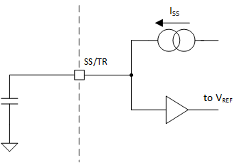
8.2.2.5.3 Soft-Start Capacitor
A capacitor connected between SS/TR pin and GND allows a user-programmable start-up slope of the output voltage.
 Figure 8-2 Soft-Start Operation Simplified
Schematic
Figure 8-2 Soft-Start Operation Simplified
SchematicAn internal constant current source is provided to charge the external capacitance. A typical soft-start ramp time is given by:
where
- CSS is the capacitance required at the SS/TR pin, the unit is pF.
- TSS is the desired soft-start ramp time, the unit is µs.
- ISS is the SS/TR source current, the unit is µA, see the Electrical Characteristics
- VREF is the feedback regulation voltage (VFB/0.75), the unit is V, see the Electrical Characteristics
The fastest achievable typical ramp time is 150 µs, even if the external Css capacitance is lower than 680 pF or the pin is open. Generally, lower than 1 ms soft-start time is not recommanded for low inrush current.
The soft-start time has variation, for more accurate configuration, the below maximum and minimum formula need to be taken into consideration.
where K is the related to the value of CSS, the unit is µs, the relationship curve is shown in Figure 8-3 and Figure 8-4.
 Figure 8-3 Relationship curve of K and Css (680pF-4800pF)
 Figure 8-4 Relationship curve of K and Css (4800pF-114000pF)