SLVSEK4C July 2019 – February 2020 TPS63810 , TPS63811
PRODUCTION DATA.
- 1 Features
- 2 Applications
- 3 Description
- 4 Revision History
- 5 Device Comparison Table
- 6 Pin Configuration and Functions
- 7 Specifications
-
8 Detailed Description
- 8.1 Overview
- 8.2 Functional Block Diagram
- 8.3
Feature Description
- 8.3.1 Control Scheme
- 8.3.2 Control Scheme
- 8.3.3 Power-Save Mode Operation (PSM)
- 8.3.4 Forced-PWM Operation (FPWM)
- 8.3.5 Ramp-PWM Operation (RPWM)
- 8.3.6 Device Enable (EN)
- 8.3.7 Undervoltage Lockout (UVLO)
- 8.3.8 Soft Start
- 8.3.9 Output Voltage Control
- 8.3.10 Protection Functions
- 8.3.11 Power Good
- 8.3.12 Load Disconnect
- 8.3.13 Output Discharge
- 8.4 Device Functional Modes
- 8.5 Programming
- 8.6
Register Map
- 8.6.1
Register Description
- 8.6.1.1 Register Map
- 8.6.1.2 Register CONTROL (Slave address: 0b1110101; Register address: 0x01; Default: 0x00 or 0x20)
- 8.6.1.3 Register STATUS (Slave address: 0b1110101; Register address: 0x02; Default: 0x00)
- 8.6.1.4 Register DEVID (Slave address: 0b1110101; Register address: 0x03; Default: 0x04)
- 8.6.1.5 Register VOUT1 (Slave address: 0b1110101; Register address: 0x04; Default: 0x3C)
- 8.6.1.6 Register VOUT2 (Slave address: 0b1110101; Register address: 0x05; Default: 0x42)
- 8.6.1
Register Description
- 9 Application and Implementation
- 10Power Supply Recommendations
- 11Layout
- 12Device and Documentation Support
- 13Mechanical, Packaging, and Orderable Information
Package Options
Mechanical Data (Package|Pins)
- YFF|15
Thermal pad, mechanical data (Package|Pins)
Orderable Information
8.3.9.1 Dynamic Voltage Scaling
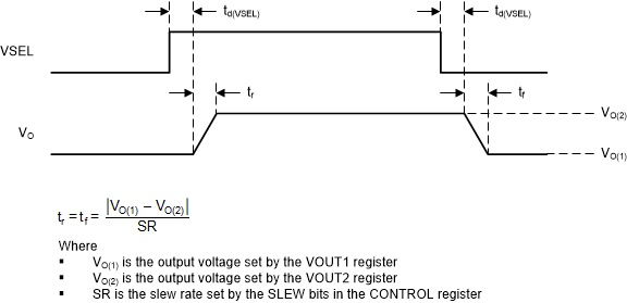
The device has a dynamic voltage scaling (DVS) function which lets you change the output voltage in a controlled way during operation. Figure 16 shows a simplified block diagram of the DVS function. The VSEL pin controls a multiplexer which selects either the VOUT1 register or the VOUT2 register to control the set voltage. The ramp control block detects when the target output voltage is different from the actual output voltage and ramps the output voltage to the target voltage in 25-mV steps. You can use the 2-bit SLEW parameter in the Control register to select one of four slew rates from 0.5 V/ms to 10 V/ms.
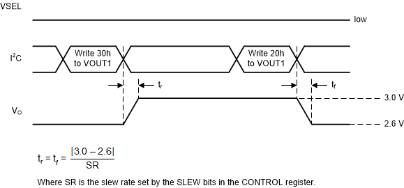
The device starts a DVS ramp when you change the logic level on the VSEL pin or program to a new value in the active VOUT register.
WHITESPACE
 Figure 16. Dynamic Voltage Scaling Block Diagram
 Note that if you change the contents of the active VOUT register or change the state of the VSEL pin during start-up (that is, before the end of the soft start), the converter uses the new value immediately and does not ramp gradually to the final value.
Figure 17 shows the timing diagram when you use the VSEL pin to change between the output voltage values in the VOUT1 and VOUT2 registers.
WHITESPACE
 Figure 17. DVS Timing Diagram Using the VSEL Pin
 WHITESPACE
Figure 18 shows the timing diagram when you use the I2C interface to change the output voltage value in one of the VOUT registers.
WHITESPACE
 Figure 18. DVS Timing Using the I2C Interface