SLVS950I July 2009 – May 2018 TPS65070 , TPS65072 , TPS65073 , TPS650731 , TPS650732
UNLESS OTHERWISE NOTED, this document contains PRODUCTION DATA.
- 1 Features
- 2 Applications
- 3 Description
- 4 Revision History
- 5 Description (continued)
- 6 Device Options
- 7 Pin Configuration and Functions
-
8 Specifications
- 8.1 Absolute Maximum Ratings
- 8.2 ESD Ratings
- 8.3 Recommended Operating Conditions
- 8.4 Thermal Information
- 8.5 Electrical Characteristics
- 8.6 Electrical Characteristics - DCDC1 Converter
- 8.7 Electrical Characteristics - DCDC2 Converter
- 8.8 Electrical Characteristics - DCDC3 Converter
- 8.9 Electrical Characteristics - VLDO1 and VLDO2 Low Dropout Regulators
- 8.10 Electrical Characteristics - wLED Boost Converter
- 8.11 Electrical Characteristics - Reset, PB_IN, PB_OUT, PGood, Power_on, INT, EN_EXTLDO, EN_wLED
- 8.12 Electrical Characteristics - ADC Converter
- 8.13 Electrical Characteristics - Touch Screen Interface
- 8.14 Electrical Characteristics - Power Path
- 8.15 Electrical Characteristics - Battery Charger
- 8.16 Timing Requirements
- 8.17 Dissipation Ratings
- 8.18 Typical Characteristics
- 9 Parameter Measurement Information
-
10Detailed Description
- 10.1 Overview
- 10.2 Functional Block Diagram
- 10.3
Feature Description
- 10.3.1 Battery Charger and Power Path
- 10.3.2 Power Down
- 10.3.3 Power-On Reset
- 10.3.4 Power-Path Management
- 10.3.5 Battery Charging
- 10.3.6 Battery Pack Temperature Monitoring
- 10.3.7 Battery Charger State Diagram
- 10.3.8 DC-DC Converters and LDOs
- 10.3.9 Power Save Mode
- 10.3.10 Short-Circuit Protection
- 10.3.11 Enable
- 10.3.12 Short-Circuit Protection
- 10.3.13 Thermal Shutdown
- 10.4 Device Functional Modes
- 10.5 Programming
- 10.6
Register Maps
- 10.6.1 PPATH1. Register Address: 01h
- 10.6.2 INT. Register Address: 02h
- 10.6.3 CHGCONFIG0. Register Address: 03h
- 10.6.4 CHGCONFIG1. Register Address: 04h
- 10.6.5 CHGCONFIG2. Register Address: 05h
- 10.6.6 CHGCONFIG3. Register Address: 06h
- 10.6.7 ADCONFIG. Register Address: 07h
- 10.6.8 TSCMODE. Register Address: 08h
- 10.6.9 ADRESULT_1. Register Address: 09h
- 10.6.10 ADRESULT_2. Register Address: 0Ah
- 10.6.11 PGOOD. Register Address: 0Bh
- 10.6.12 PGOODMASK. Register Address: 0Ch
- 10.6.13 CON_CTRL1. Register Address: 0Dh
- 10.6.14 CON_CTRL2. Register Address: 0Eh
- 10.6.15 CON_CTRL3. Register Address: 0Fh
- 10.6.16 DEFDCDC1. Register Address: 10h
- 10.6.17 DEFDCDC2_LOW. Register Address: 11h
- 10.6.18 DEFDCDC2_HIGH. Register Address: 12h
- 10.6.19 DEFDCDC3_LOW. Register Address: 13h
- 10.6.20 DEFDCDC3_HIGH. Register Address: 14h
- 10.6.21 DEFSLEW. Register Address: 15h
- 10.6.22 LDO_CTRL1. Register Address: 16h
- 10.6.23 DEFLDO2. Register Address: 17h
- 10.6.24 WLED_CTRL1. Register Address: 18h
- 10.6.25 WLED_CTRL2. Register Address: 19h
-
11Application and Implementation
- 11.1 Application Information
- 11.2
Typical Applications
- 11.2.1 General PMIC Application
- 11.2.2 Powering OMAP-L138
- 11.2.3 Powering Atlas IV
- 11.2.4 OMAP35xx (Supporting SYS-OFF Mode)
- 11.2.5 TPS650731 for OMAP35xx
- 11.2.6 Powering AM3505 Using TPS650732
- 12Power Supply Recommendations
- 13Layout
- 14Device and Documentation Support
- 15Mechanical, Packaging, and Orderable Information
Package Options
Mechanical Data (Package|Pins)
- RSL|48
Thermal pad, mechanical data (Package|Pins)
- RSL|48
Orderable Information
10.3.11.3 PB_IN (Push-Button IN)
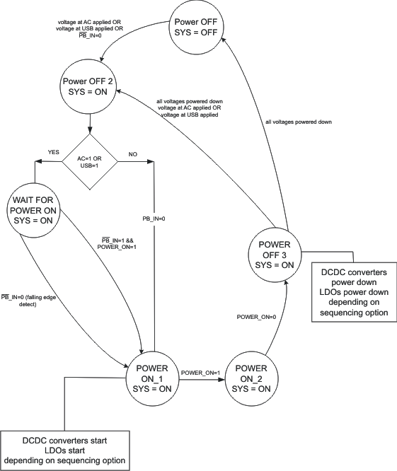
This pin is the ON/OFF button for the PMU to leave OFF-state and enter ON-state by pulling this pin to GND. Entering ON-state will first ramp the output voltage of the power path (SYS), load the default register settings and start up the DCDC converters and LDOs with the sequencing defined. In ON-state, the I2C interface is active and the wLED converter can be enabled. The system turns on if PB_IN is pulled LOW for >50 ms (debounce time) AND the output voltage of the power path manager is above the undervoltage lockout voltage (AVDD6 > 3 V). This is for Vbat>3 V OR VAC>3 V OR VUSB>3 V. The default voltage for the undervoltage lockout voltage can be changed with Bits <UVLO1>, <UVLO0> in register CON_CTRL2. The value will be valid until the device was turned off completely by entering Off state. The system turns off if PB_IN is released OR the system voltage falls below the undervoltage lockout voltage of 3 V. This is the case when either the battery voltage drops below 3 V or the input voltage at the pins AC or USB is below 3 V. In order to keep the TPS6507x enabled after PB_IN is released HIGH, there is an input pin called POWER_ON which needs to be pulled HIGH before the PB_IN button is released. POWER_ON=HIGH will typically be asserted by the application processor to keep the PMU in ON-state after the power button at PB_IN is released.
In addition to this, there is a 15-s timer which will drive PGOOD=LOW for 0.5 ms when 15 s are expired. The 15-s timer is enabled again when PB_IN is released HIGH. If PB_IN is pulled LOW for 30 s continuously, PGOOD will be driven LOW only once after the first 15 s. When PGOOD is driven LOW due to PB_IN=low for 15 s, all registers in TPS6507x are set to their default value. See Figure 34.
 Figure 34. State Machine