SLVS950I July 2009 – May 2018 TPS65070 , TPS65072 , TPS65073 , TPS650731 , TPS650732
UNLESS OTHERWISE NOTED, this document contains PRODUCTION DATA.
- 1 Features
- 2 Applications
- 3 Description
- 4 Revision History
- 5 Description (continued)
- 6 Device Options
- 7 Pin Configuration and Functions
-
8 Specifications
- 8.1 Absolute Maximum Ratings
- 8.2 ESD Ratings
- 8.3 Recommended Operating Conditions
- 8.4 Thermal Information
- 8.5 Electrical Characteristics
- 8.6 Electrical Characteristics - DCDC1 Converter
- 8.7 Electrical Characteristics - DCDC2 Converter
- 8.8 Electrical Characteristics - DCDC3 Converter
- 8.9 Electrical Characteristics - VLDO1 and VLDO2 Low Dropout Regulators
- 8.10 Electrical Characteristics - wLED Boost Converter
- 8.11 Electrical Characteristics - Reset, PB_IN, PB_OUT, PGood, Power_on, INT, EN_EXTLDO, EN_wLED
- 8.12 Electrical Characteristics - ADC Converter
- 8.13 Electrical Characteristics - Touch Screen Interface
- 8.14 Electrical Characteristics - Power Path
- 8.15 Electrical Characteristics - Battery Charger
- 8.16 Timing Requirements
- 8.17 Dissipation Ratings
- 8.18 Typical Characteristics
- 9 Parameter Measurement Information
-
10Detailed Description
- 10.1 Overview
- 10.2 Functional Block Diagram
- 10.3
Feature Description
- 10.3.1 Battery Charger and Power Path
- 10.3.2 Power Down
- 10.3.3 Power-On Reset
- 10.3.4 Power-Path Management
- 10.3.5 Battery Charging
- 10.3.6 Battery Pack Temperature Monitoring
- 10.3.7 Battery Charger State Diagram
- 10.3.8 DC-DC Converters and LDOs
- 10.3.9 Power Save Mode
- 10.3.10 Short-Circuit Protection
- 10.3.11 Enable
- 10.3.12 Short-Circuit Protection
- 10.3.13 Thermal Shutdown
- 10.4 Device Functional Modes
- 10.5 Programming
- 10.6
Register Maps
- 10.6.1 PPATH1. Register Address: 01h
- 10.6.2 INT. Register Address: 02h
- 10.6.3 CHGCONFIG0. Register Address: 03h
- 10.6.4 CHGCONFIG1. Register Address: 04h
- 10.6.5 CHGCONFIG2. Register Address: 05h
- 10.6.6 CHGCONFIG3. Register Address: 06h
- 10.6.7 ADCONFIG. Register Address: 07h
- 10.6.8 TSCMODE. Register Address: 08h
- 10.6.9 ADRESULT_1. Register Address: 09h
- 10.6.10 ADRESULT_2. Register Address: 0Ah
- 10.6.11 PGOOD. Register Address: 0Bh
- 10.6.12 PGOODMASK. Register Address: 0Ch
- 10.6.13 CON_CTRL1. Register Address: 0Dh
- 10.6.14 CON_CTRL2. Register Address: 0Eh
- 10.6.15 CON_CTRL3. Register Address: 0Fh
- 10.6.16 DEFDCDC1. Register Address: 10h
- 10.6.17 DEFDCDC2_LOW. Register Address: 11h
- 10.6.18 DEFDCDC2_HIGH. Register Address: 12h
- 10.6.19 DEFDCDC3_LOW. Register Address: 13h
- 10.6.20 DEFDCDC3_HIGH. Register Address: 14h
- 10.6.21 DEFSLEW. Register Address: 15h
- 10.6.22 LDO_CTRL1. Register Address: 16h
- 10.6.23 DEFLDO2. Register Address: 17h
- 10.6.24 WLED_CTRL1. Register Address: 18h
- 10.6.25 WLED_CTRL2. Register Address: 19h
-
11Application and Implementation
- 11.1 Application Information
- 11.2
Typical Applications
- 11.2.1 General PMIC Application
- 11.2.2 Powering OMAP-L138
- 11.2.3 Powering Atlas IV
- 11.2.4 OMAP35xx (Supporting SYS-OFF Mode)
- 11.2.5 TPS650731 for OMAP35xx
- 11.2.6 Powering AM3505 Using TPS650732
- 12Power Supply Recommendations
- 13Layout
- 14Device and Documentation Support
- 15Mechanical, Packaging, and Orderable Information
Package Options
Mechanical Data (Package|Pins)
- RSL|48
Thermal pad, mechanical data (Package|Pins)
- RSL|48
Orderable Information
10.3.13.4.1 Performing Measurements Using the Touch Screen Controller
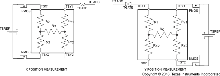
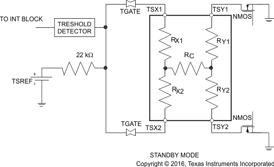
To take measurements with the touch screen controller, the ADC has to be enabled and configured for use with the touch screen controller (TSC) first. In case the TSC is planned to be operated interrupt driven, the TSC needs to be in TSC standby mode per default. Only in TSC standby mode an interrupt is generated based on a touch of the screen. The TSC should therefore be in this mode until a touch is detected. Afterwards, the TSC has to be configured for x-position measurement followed by y-position measurement. Now, the TSC can be set to TSC standby again to wait for the next touch of the screen. For a non-interrupt driven sequence, see TSCMODE. Register Address: 08h (page 50) in the Registers section. A typical interrupt driven sequence is given below:
- Set TSCMODE to 101 to set TSC to TSC standby, so an interrupt is generated when the screen is touched
- Set Bit AD enable = 1 to provide power to the ADC
- Set input select for the ADC in register ADCONFIG to 1110 (AD_IN14 selected)
- In register INT, set MASK TSC = 1 to unmask the interrupt on a touch of the touch screen
- Read Bit TSC INT as it will be set after the TSC has been configured. Reading clears the interrupt.
- After a touch was detected, an interrupt is generated by INT pin going LOW
- Read Bit TSC INT to clear the interrupt
- Set TSCMODE to 000 to select x-position measurement
- Start an ADC conversion by setting CONVERSION START =1; wait until END OF CONVERSION = 1
- Read register ADRESULT_1 and AD_RESULT_2
- Set TSCMODE to 001 to select y-position measurement
- Start an ADC conversion by setting CONVERSION START =1; wait until END OF CONVERSION = 1
- Read register ADRESULT_1 and AD_RESULT_2
- Set TSCMODE to 101 to set TSC to TSC standby again
 Figure 36. Two Position Measurement
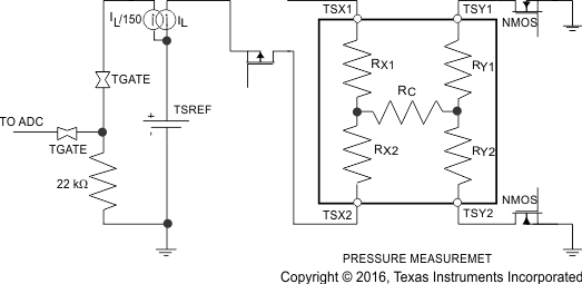
 Figure 37. Pressure Measurement
 Figure 38. Two Plate Resistance Measurement
 Figure 39. Touch Screen Standby Mode