SBVS054K November   2004  – June 2025 TPS730

PRODUCTION DATA  

  1.   1
  2. Features
  3. Applications
  4. Description
  5. Pin Configuration and Functions
  6. Specifications
    1. 5.1 Absolute Maximum Ratings
    2. 5.2 ESD Ratings
    3. 5.3 Recommended Operating Conditions
    4. 5.4 Thermal Information
    5. 5.5 Electrical Characteristics
    6. 5.6 Typical Characteristics
  7. Detailed Description
    1. 6.1 Overview
    2. 6.2 Functional Block Diagrams
    3. 6.3 Feature Description
      1. 6.3.1 Undervoltage Lockout (UVLO)
      2. 6.3.2 Shutdown
      3. 6.3.3 Foldback Current Limit
    4. 6.4 Device Functional Modes
      1. 6.4.1 Normal Operation
      2. 6.4.2 Dropout Operation
      3. 6.4.3 Disabled
  8. Application and Implementation
    1. 7.1 Application Information
      1. 7.1.1 Adjustable Operation
      2. 7.1.2 Capacitor Recommendations
      3. 7.1.3 Input and Output Capacitor Requirements
      4. 7.1.4 Noise-Reduction and Feed-Forward Capacitor Requirements
      5. 7.1.5 Reverse Current Operation
    2. 7.2 Typical Application
      1. 7.2.1 Design Requirements
      2. 7.2.2 Detailed Design Procedure
      3. 7.2.3 Application Curves
    3. 7.3 Best Design Practices
    4. 7.4 Power Supply Recommendations
    5. 7.5 Layout
      1. 7.5.1 Layout Guidelines
        1. 7.5.1.1 Board Layout Recommendations to Improve PSRR and Noise Performance
        2. 7.5.1.2 Thermal Considerations
        3. 7.5.1.3 Power Dissipation
      2. 7.5.2 Layout Examples
  9. Device and Documentation Support
    1. 8.1 Device Support
      1. 8.1.1 Development Support
        1. 8.1.1.1 Spice Models
      2. 8.1.2 Device Nomenclature
    2. 8.2 Documentation Support
      1. 8.2.1 Related Documentation
    3. 8.3 Receiving Notification of Documentation Updates
    4. 8.4 Support Resources
    5. 8.5 Trademarks
    6. 8.6 Electrostatic Discharge Caution
    7. 8.7 Glossary
  10. Revision History
  11. 10Mechanical, Packaging, and Orderable Information
    1. 10.1 TPS730YZQ Nanostar™ Wafer Chip Scale Information

Package Options

Mechanical Data (Package|Pins)
Thermal pad, mechanical data (Package|Pins)
Orderable Information

Typical Characteristics

over recommended operating temperature range TJ = –40°C to +125°C, VEN = VIN, VIN = VOUT(nom) + 1 V, IOUT = 1 mA, COUT = 10 μF, CNR = 0.01 μF, VOUT(nom) = 2.8 V (unless otherwise noted). Typical values are at TJ = 25°C.
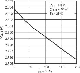
TPS730 TPS730 Output Voltage vs Output Current
Legacy chip
Figure 5-1 TPS730 Output Voltage vs Output Current
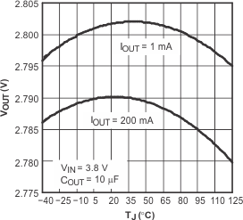
TPS730 TPS730 Output Voltage vs Junction
                                                  Temperature
Legacy chip
Figure 5-3 TPS730 Output Voltage vs Junction Temperature
TPS730 TPS730 Ground Current vs Junction
                                                  Temperature
Legacy chip
Figure 5-5 TPS730 Ground Current vs Junction Temperature
TPS730 TPS730 Output Spectral Noise Density vs
                                                  Frequency
Legacy chip
Figure 5-7 TPS730 Output Spectral Noise Density vs Frequency
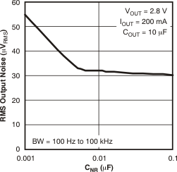
TPS730 Root Mean Square Output Noise vs
                                                  CNR
Legacy chip
Figure 5-9 Root Mean Square Output Noise vs CNR
TPS730 TPS730 Dropout Voltage vs Junction
                                                  Temperature
New chip
Figure 5-11 TPS730 Dropout Voltage vs Junction Temperature
TPS730 TPS730 Ripple Rejection vs Frequency
New chip
Figure 5-13 TPS730 Ripple Rejection vs Frequency
TPS730 TPS730 Output Voltage, Enable Voltage vs Time
                                                  (Start-Up)
Legacy chip
Figure 5-15 TPS730 Output Voltage, Enable Voltage vs Time (Start-Up)
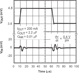
TPS730 TPS730 Line Transient Response
Legacy chip
Figure 5-17 TPS730 Line Transient Response
TPS730 TPS730 Load Transient Response
Legacy chip
Figure 5-19 TPS730 Load Transient Response
TPS730 Power-Up and Power-Down
Legacy chip
Figure 5-21 Power-Up and Power-Down
TPS730 Dropout Voltage vs Output Current
Legacy chip
Figure 5-23 Dropout Voltage vs Output Current
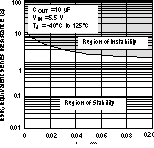
TPS730 Typical Regions of Stability Equivalent Series
                                                  Resistance (ESR) vs Output Current
Legacy chip
Figure 5-25 Typical Regions of Stability Equivalent Series Resistance (ESR) vs Output Current
TPS730 TPS730 Output Voltage vs Output Current
New chip
Figure 5-2 TPS730 Output Voltage vs Output Current
TPS730 TPS730 Output Voltage vs Junction
                                                  Temperature
New chip
Figure 5-4 TPS730 Output Voltage vs Junction Temperature
TPS730 TPS730 Ground Current vs Junction
                                                  Temperature
New chip
Figure 5-6 TPS730 Ground Current vs Junction Temperature
TPS730 TPS730 Output Spectral Noise Density vs
                                                  Frequency
COUT = 10uF (new chip)
Figure 5-8 TPS730 Output Spectral Noise Density vs Frequency
TPS730 TPS730 Dropout Voltage vs Junction
                                                  Temperature
Legacy chip
Figure 5-10 TPS730 Dropout Voltage vs Junction Temperature
TPS730 TPS730 Ripple Rejection vs Frequency
Legacy chip
Figure 5-12 TPS730 Ripple Rejection vs Frequency
TPS730 TPS730 Ripple Rejection vs Frequency
New chip
Figure 5-14 TPS730 Ripple Rejection vs Frequency
TPS730 TPS730 Output Voltage, Enable Voltage vs Time
                                                  (Start-Up)
New chip
Figure 5-16 TPS730 Output Voltage, Enable Voltage vs Time (Start-Up)
TPS730 TPS730 Line Transient Response
New chip
Figure 5-18 TPS730 Line Transient Response
TPS730 TPS730 Load Transient Response
New chip
Figure 5-20 TPS730 Load Transient Response
TPS730 Power-Up and Power-Down
New chip
Figure 5-22 Power-Up and Power-Down
TPS730 Dropout Voltage vs Output Current
New chip
Figure 5-24 Dropout Voltage vs Output Current
TPS730 Typical Regions of Stability Equivalent Series
                                                  Resistance (ESR) vs Output Current
Legacy chip
Figure 5-26 Typical Regions of Stability Equivalent Series Resistance (ESR) vs Output Current