SLVS337E March 2001 – January 2025 TPS792
PRODUCTION DATA
- 1
- 1 Features
- 2 Applications
- 3 Description
- 4 Pin Configuration and Functions
- 5 Specifications
- 6 Detailed Description
- 7 Application and Implementation
- 8 Device and Documentation Support
- 9 Revision History
- 10Mechanical, Packaging, and Orderable Information
Package Options
Mechanical Data (Package|Pins)
Thermal pad, mechanical data (Package|Pins)
Orderable Information
7.1.1 Adjustable Operation
The output voltage of the TPS792xx01 adjustable regulator is programmed using an external resistor divider as shown in the image below. The output voltage is calculated using the equation below:
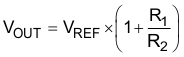
where:
- VREF = 1.2246V typ (the internal reference voltage)
Resistors R1 and R2 must be selected for approximately 50μA divider current. Lower value resistors can be used for improved noise performance, but the solution consumes more power. Higher resistors values can cause accuracy issues and other problems. The recommended design procedure is to choose R2 = 30.1kΩ to set the divider current at 50μA, CFF = 15pF for stability, and then calculate R1 using the equation below:

To improve the stability of the adjustable version, place a small compensation capacitor between OUT and FB. For output voltages less than 1.8V, the value of this capacitor must be 100pF. For output voltages greater than 1.8V, the approximate value of this capacitor can be calculated as shown in the equation below:
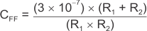
The suggested value of this capacitor for several resistor ratios is shown in the table in the image below. If this capacitor is not used (such as in a unity-gain configuration) or if an output voltage less than 1.8V is chosen, then the minimum recommended output capacitor is 4.7μF instead of 2.2μF.

| OUTPUT VOLTAGE | R1 | R2 | CFF |
|---|---|---|---|
| 1.22V | Short | Open | 0pF |
| 2.5V | 31.6kΩ | 30.1kΩ | 22pF |
| 3.3V | 51kΩ | 30.1kΩ | 15pF |
| 3.6V | 59kΩ | 30.1kΩ | 15pF |