SLVS337E March   2001  â€“ January 2025 TPS792

PRODUCTION DATA  

  1.   1
  2. Features
  3. Applications
  4. Description
  5. Pin Configuration and Functions
  6. Specifications
    1. 5.1 Absolute Maximum Ratings
    2. 5.2 ESD Ratings
    3. 5.3 Recommended Operating Conditions
    4. 5.4 Thermal Information
    5. 5.5 Electrical Characteristics
    6. 5.6 Typical Characteristics
  7. Detailed Description
    1. 6.1 Overview
    2. 6.2 Functional Block Diagrams
    3. 6.3 Feature Description
      1. 6.3.1 Undervoltage Lockout (UVLO)
      2. 6.3.2 Shutdown
      3. 6.3.3 Active Discharge (New Chip)
      4. 6.3.4 Foldback Current Limit
      5. 6.3.5 Thermal Protection
      6. 6.3.6 Reverse Current
    4. 6.4 Device Functional Modes
      1. 6.4.1 Normal Operation
      2. 6.4.2 Dropout Operation
      3. 6.4.3 Disabled
  8. Application and Implementation
    1. 7.1 Application Information
      1. 7.1.1 Adjustable Operation
      2. 7.1.2 Exiting Dropout
    2. 7.2 Typical Application
      1. 7.2.1 Design Requirements
      2. 7.2.2 Detailed Design Procedure
        1. 7.2.2.1 Capacitor Recommendations
        2. 7.2.2.2 Input and Output Capacitor Requirements
        3. 7.2.2.3 Noise Reduction and Feed-Forward Capacitor Requirements
      3. 7.2.3 Application Curves
    3. 7.3 Power Supply Recommendations
    4. 7.4 Layout
      1. 7.4.1 Layout Guidelines
        1. 7.4.1.1 Board Layout Recommendations to Improve PSRR and Noise Performance
        2. 7.4.1.2 Power Dissipation and Junction Temperature
      2. 7.4.2 Layout Example
  9. Device and Documentation Support
    1. 8.1 Device Support
      1. 8.1.1 Development Support
        1. 8.1.1.1 Evaluation Modules
        2. 8.1.1.2 Spice Models
      2. 8.1.2 Device Nomenclature
    2. 8.2 Documentation Support
      1. 8.2.1 Related Documentation
    3. 8.3 Receiving Notification of Documentation Updates
    4. 8.4 Support Resources
    5. 8.5 Trademarks
    6. 8.6 Electrostatic Discharge Caution
    7. 8.7 Glossary
  10. Revision History
  11. 10Mechanical, Packaging, and Orderable Information

Package Options

Mechanical Data (Package|Pins)
Thermal pad, mechanical data (Package|Pins)
Orderable Information

Typical Characteristics

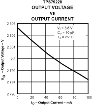
TPS792 TPS792 Output
                                    Voltage vs Output Current
Legacy chip
Figure 5-1 TPS792 Output Voltage vs Output Current
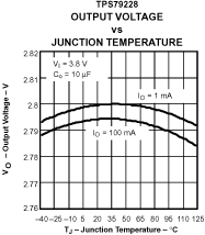
TPS792 TPS792 Output
                                    Voltage vs Junction Temperature
Legacy chip
Figure 5-3 TPS792 Output Voltage vs Junction Temperature
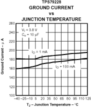
TPS792 TPS792 Ground
                                    Current vs Junction Temperature
Legacy chip
Figure 5-5 TPS792 Ground Current vs Junction Temperature
TPS792 TPS792 Output
                                    Spectral Noise Density vs Frequency
Legacy chip
Figure 5-7 TPS792 Output Spectral Noise Density vs Frequency
TPS792 TPS792 Output
                                    Spectral Noise Density vs Frequency
Legacy chip
Figure 5-9 TPS792 Output Spectral Noise Density vs Frequency
TPS792 Root Mean Squared
                                    Output Noise vs Bypass Capacitance
Legacy chip
Figure 5-11 Root Mean Squared Output Noise vs Bypass Capacitance
TPS792 Output Impedance
                                    vs Frequency
New chip
Figure 5-13 Output Impedance vs Frequency
TPS792 TPS792 Dropout
                                    Voltage vs Junction Temperature
New chip
Figure 5-15 TPS792 Dropout Voltage vs Junction Temperature
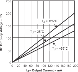
TPS792 Dropout Voltage
                                    vs Output Current
New chip
Figure 5-17 Dropout Voltage vs Output Current
TPS792 TPS792 Dropout
                                    Voltage vs Input Voltage
New chip
Figure 5-19 TPS792 Dropout Voltage vs Input Voltage
TPS792 TPS792 Ripple
                                    Rejection vs Frequency
Legacy chip
Figure 5-21 TPS792 Ripple Rejection vs Frequency
TPS792 TPS792 Ripple
                                    Rejection vs Frequency
Legacy chip
Figure 5-23 TPS792 Ripple Rejection vs Frequency
TPS792 TPS792 Ripple
                                    Rejection vs Frequency
New chip
Figure 5-25 TPS792 Ripple Rejection vs Frequency
TPS792 TPS792 Output
                                    Voltage and Enable Voltage vs Time (Start-Up)
New chip
Figure 5-27 TPS792 Output Voltage and Enable Voltage vs Time (Start-Up)
TPS792 TPS792 Line
                                    Transient Response
New chip
Figure 5-29 TPS792 Line Transient Response
TPS792 TPS792 Load
                                    Transient Response
New chip
Figure 5-31 TPS792 Load Transient Response
TPS792 Typical Regions
                                    of Stability Equivalent Series Resistance (ESR) vs Output
                                    Current
Legacy chip
Figure 5-33 Typical Regions of Stability Equivalent Series Resistance (ESR) vs Output Current
TPS792 TPS792 Output
                                    Voltage vs Output Current
New chip
Figure 5-2 TPS792 Output Voltage vs Output Current
TPS792 TPS792 Output
                                    Voltage vs Junction Temperature
New chip
Figure 5-4 TPS792 Output Voltage vs Junction Temperature
TPS792 TPS792 Ground
                                    Current vs IOUT
New chip
Figure 5-6 TPS792 Ground Current vs IOUT
TPS792 TPS792 Output
                                    Spectral Noise Density vs Frequency
Legacy chip
Figure 5-8 TPS792 Output Spectral Noise Density vs Frequency
TPS792 TPS792 Output
                                    Spectral Noise Density vs Frequency
New chip
Figure 5-10 TPS792 Output Spectral Noise Density vs Frequency
TPS792 Output Impedance
                                    vs Frequency
Legacy chip
Figure 5-12 Output Impedance vs Frequency
TPS792 TPS792 Dropout
                                    Voltage vs Junction Temperature
Legacy chip
Figure 5-14 TPS792 Dropout Voltage vs Junction Temperature
TPS792 Dropout Voltage
                                    vs Output Current
Legacy chip
Figure 5-16 Dropout Voltage vs Output Current
TPS792 TPS792 Dropout
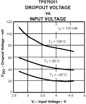
                                    Voltage vs Input Voltage
Legacy chip
Figure 5-18 TPS792 Dropout Voltage vs Input Voltage
TPS792 Minimum Required
                                    Input Voltage vs Output Voltage
Legacy chip
Figure 5-20 Minimum Required Input Voltage vs Output Voltage
TPS792 TPS792 Ripple
                                    Rejection vs Frequency
New chip
Figure 5-22 TPS792 Ripple Rejection vs Frequency
TPS792 TPS792 Ripple
                                    Rejection vs Frequency
Legacy chip
Figure 5-24 TPS792 Ripple Rejection vs Frequency
TPS792 TPS792 Output
                                    Voltage and Enable Voltage vs Time (Start-Up)
Legacy chip
Figure 5-26 TPS792 Output Voltage and Enable Voltage vs Time (Start-Up)
TPS792 TPS792 Line
                                    Transient Response
Legacy chip
Figure 5-28 TPS792 Line Transient Response
TPS792 TPS792 Load
                                    Transient Response
Legacy chip
Figure 5-30 TPS792 Load Transient Response
TPS792 Typical Regions
                                    of Stability Equivalent Series Resistance (ESR) vs Output
                                    Current
Legacy chip
Figure 5-32 Typical Regions of Stability Equivalent Series Resistance (ESR) vs Output Current
TPS792 Typical Regions
                                    of Stability Equivalent Series Resistance (ESR) vs Output
                                    Current
Legacy chip
Figure 5-34 Typical Regions of Stability Equivalent Series Resistance (ESR) vs Output Current