SLUSCX8C March 2019 – March 2021 TPS92682-Q1
PRODUCTION DATA
- 1 Features
- 2 Applications
- 3 Description
- 4 Revision History
- 5 Pin Configuration and Functions
- 6 Specifications
-
7 Detailed Description
- 7.1 Overview
- 7.2 Functional Block Diagram
- 7.3
Feature Description
- 7.3.1 Device Enable
- 7.3.2 Internal Regulator and Undervoltage Lockout (UVLO)
- 7.3.3 Oscillator
- 7.3.4 Spread Spectrum Function
- 7.3.5 Gate Driver
- 7.3.6 Rail-to-Rail Current Sense Amplifier
- 7.3.7 Transconductance Error Amplifier
- 7.3.8 Switch Current Sense
- 7.3.9 Slope Compensation
- 7.3.10 ILED Setting in CC Mode
- 7.3.11 Output Voltage Setting in CV Mode
- 7.3.12 PWM Dimming
- 7.3.13 P-Channel FET Gate Driver Output
- 7.3.14 Soft Start
- 7.3.15 Two-Phase Operation
- 7.3.16 Faults and Diagnostics
- 7.4 Device Functional Modes
- 7.5 Programming
- 7.6
TPS92682 Registers
- 7.6.1 EN Register
- 7.6.2 CFG1 Register
- 7.6.3 CFG2 Register
- 7.6.4 SWDIV Register
- 7.6.5 ISLOPE Register
- 7.6.6 FM Register
- 7.6.7 SOFTSTART Register
- 7.6.8 CH1IADJ Register
- 7.6.9 CH2IADJ Register
- 7.6.10 PWMDIV Register
- 7.6.11 CH1PWML Register
- 7.6.12 CH1PWMH Register
- 7.6.13 CH2PWML Register
- 7.6.14 CH2PWMH Register
- 7.6.15 ILIM Register
- 7.6.16 IFT Register
- 7.6.17 MFT Register
- 7.6.18 FLT1 Register (read only)
- 7.6.19 FLT2 Register (read only)
- 7.6.20 FEN1 Register
- 7.6.21 FEN2 Register
- 7.6.22 FLATEN Register
- 7.6.23 OV Register
- 7.6.24 LHCFG Register
- 7.6.25 LHCH1IADJ Register
- 7.6.26 LHCH2IADJ Register
- 7.6.27 LHCH1PWML Register
- 7.6.28 LHCH1PWMH Register
- 7.6.29 LHCH2PWML Register
- 7.6.30 LHCH2PWMH Register
- 7.6.31 LHILIM Register
- 7.6.32 LHIFT Register
- 7.6.33 LHMFT Register
- 7.6.34 LHFEN1 Register
- 7.6.35 LHFEN2 Register
- 7.6.36 LHFLATEN Register
- 7.6.37 LHOV Register
- 7.6.38 CAL Register
- 7.6.39 RESET Register
-
8 Application and Implementation
- 8.1 Application Information General Design Considerations
- 8.2 Application Information CC Mode
- 8.3 Typical Application CV Mode
- 8.4
Typical Application CC Mode
- 8.4.1 CC Boost Design Requirements
- 8.4.2
CC Boost Detailed Design Procedure
- 8.4.2.1 Calculating Duty Cycle
- 8.4.2.2 Setting Switching Frequency
- 8.4.2.3 Setting Dither Modulation Frequency
- 8.4.2.4 Inductor Selection
- 8.4.2.5 Output Capacitor Selection
- 8.4.2.6 Input Capacitor Selection
- 8.4.2.7 Main N-Channel MOSFET Selection
- 8.4.2.8 Rectifier Diode Selection
- 8.4.2.9 Setting ILED and Selecting RCS
- 8.4.2.10 Setting Switch Current Limit
- 8.4.2.11 Slope Compensation
- 8.4.2.12 Compensator Parameters
- 8.4.2.13 Overvoltage Protection
- 8.4.2.14 Series P-Channel MOSFET Selection
- 8.4.3 CC Buck-Boost Design Requirements
- 8.4.4
CC Buck-Boost Detailed Design Procedure
- 8.4.4.1 Calculating Duty Cycle
- 8.4.4.2 Setting Switching Frequency
- 8.4.4.3 Setting Dither Modulation Frequency
- 8.4.4.4 Inductor Selection
- 8.4.4.5 Output Capacitor Selection
- 8.4.4.6 Input Capacitor Selection
- 8.4.4.7 Main N-Channel MOSFET Selection
- 8.4.4.8 Rectifier Diode Selection
- 8.4.4.9 Setting ILED and Selecting RCS
- 8.4.4.10 Setting Switch Current Limit
- 8.4.4.11 Slope Compensation
- 8.4.4.12 Compensator Parameters
- 8.4.4.13 Overvoltage Protection
- 8.4.5 PWM Dimming Consideration
- 8.4.6 Application Curves
- 8.5
Typical Application CV Mode
- 8.5.1 CV Design Requirements
- 8.5.2
Detailed Design Procedure
- 8.5.2.1 Calculating Duty Cycle
- 8.5.2.2 Setting Switching Frequency
- 8.5.2.3 Setting Dither Modulation Frequency
- 8.5.2.4 Inductor Selection
- 8.5.2.5 Output Capacitor Selection
- 8.5.2.6 Input Capacitor Selection
- 8.5.2.7 Main N-Channel MOSFET Selection
- 8.5.2.8 Rectifier Diode Selection
- 8.5.2.9 Programming VOUT
- 8.5.2.10 Setting Switch Current Limit
- 8.5.2.11 Slope Compensation
- 8.5.2.12 Compensator Parameters
- 8.5.2.13 Overvoltage Protection
- 8.5.3 Application Curves
- 9 Power Supply Recommendations
- 10Layout
- 11Device and Documentation Support
- 12Mechanical, Packaging, and Orderable Information
Package Options
Mechanical Data (Package|Pins)
Thermal pad, mechanical data (Package|Pins)
Orderable Information
8.2.2 Output Capacitor Selection
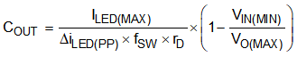
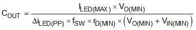
The output capacitors are required to attenuate the discontinuous or large ripple output current, and achieve the desired peak-to-peak LED current ripple, ΔiLED(PP). The capacitor value depends on the total series resistance of the LED string, rD, and the switching frequency, fSW.The capacitance required for the target LED ripple current can be calculated based on following equations.
Boost:
Buck-Boost:
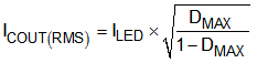
When choosing the output capacitors, it is important to consider the ESR and the ESL characteristics as they directly impact the LED current ripple. Ceramic capacitors are the best choice due to their low ESR, high ripple current rating, long lifetime, and good temperature performance. When selecting ceramic capacitors, it is important to consider the derating factors associated with higher temperature and the DC bias operating conditions. TI recommends an X7R dielectric with voltage rating greater than maximum LED stack voltage. An aluminum electrolytic capacitor can be used in parallel with ceramic capacitors to provide bulk energy storage. The aluminum capacitors must have necessary RMS current and temperature ratings to ensure prolonged operating lifetime. The minimum allowable RMS output capacitor current rating, ICOUT(RMS), can be approximated as:
Boost and Buck-Boost: