SLUSCX8C March 2019 – March 2021 TPS92682-Q1
PRODUCTION DATA
- 1 Features
- 2 Applications
- 3 Description
- 4 Revision History
- 5 Pin Configuration and Functions
- 6 Specifications
-
7 Detailed Description
- 7.1 Overview
- 7.2 Functional Block Diagram
- 7.3
Feature Description
- 7.3.1 Device Enable
- 7.3.2 Internal Regulator and Undervoltage Lockout (UVLO)
- 7.3.3 Oscillator
- 7.3.4 Spread Spectrum Function
- 7.3.5 Gate Driver
- 7.3.6 Rail-to-Rail Current Sense Amplifier
- 7.3.7 Transconductance Error Amplifier
- 7.3.8 Switch Current Sense
- 7.3.9 Slope Compensation
- 7.3.10 ILED Setting in CC Mode
- 7.3.11 Output Voltage Setting in CV Mode
- 7.3.12 PWM Dimming
- 7.3.13 P-Channel FET Gate Driver Output
- 7.3.14 Soft Start
- 7.3.15 Two-Phase Operation
- 7.3.16 Faults and Diagnostics
- 7.4 Device Functional Modes
- 7.5 Programming
- 7.6
TPS92682 Registers
- 7.6.1 EN Register
- 7.6.2 CFG1 Register
- 7.6.3 CFG2 Register
- 7.6.4 SWDIV Register
- 7.6.5 ISLOPE Register
- 7.6.6 FM Register
- 7.6.7 SOFTSTART Register
- 7.6.8 CH1IADJ Register
- 7.6.9 CH2IADJ Register
- 7.6.10 PWMDIV Register
- 7.6.11 CH1PWML Register
- 7.6.12 CH1PWMH Register
- 7.6.13 CH2PWML Register
- 7.6.14 CH2PWMH Register
- 7.6.15 ILIM Register
- 7.6.16 IFT Register
- 7.6.17 MFT Register
- 7.6.18 FLT1 Register (read only)
- 7.6.19 FLT2 Register (read only)
- 7.6.20 FEN1 Register
- 7.6.21 FEN2 Register
- 7.6.22 FLATEN Register
- 7.6.23 OV Register
- 7.6.24 LHCFG Register
- 7.6.25 LHCH1IADJ Register
- 7.6.26 LHCH2IADJ Register
- 7.6.27 LHCH1PWML Register
- 7.6.28 LHCH1PWMH Register
- 7.6.29 LHCH2PWML Register
- 7.6.30 LHCH2PWMH Register
- 7.6.31 LHILIM Register
- 7.6.32 LHIFT Register
- 7.6.33 LHMFT Register
- 7.6.34 LHFEN1 Register
- 7.6.35 LHFEN2 Register
- 7.6.36 LHFLATEN Register
- 7.6.37 LHOV Register
- 7.6.38 CAL Register
- 7.6.39 RESET Register
-
8 Application and Implementation
- 8.1 Application Information General Design Considerations
- 8.2 Application Information CC Mode
- 8.3 Typical Application CV Mode
- 8.4
Typical Application CC Mode
- 8.4.1 CC Boost Design Requirements
- 8.4.2
CC Boost Detailed Design Procedure
- 8.4.2.1 Calculating Duty Cycle
- 8.4.2.2 Setting Switching Frequency
- 8.4.2.3 Setting Dither Modulation Frequency
- 8.4.2.4 Inductor Selection
- 8.4.2.5 Output Capacitor Selection
- 8.4.2.6 Input Capacitor Selection
- 8.4.2.7 Main N-Channel MOSFET Selection
- 8.4.2.8 Rectifier Diode Selection
- 8.4.2.9 Setting ILED and Selecting RCS
- 8.4.2.10 Setting Switch Current Limit
- 8.4.2.11 Slope Compensation
- 8.4.2.12 Compensator Parameters
- 8.4.2.13 Overvoltage Protection
- 8.4.2.14 Series P-Channel MOSFET Selection
- 8.4.3 CC Buck-Boost Design Requirements
- 8.4.4
CC Buck-Boost Detailed Design Procedure
- 8.4.4.1 Calculating Duty Cycle
- 8.4.4.2 Setting Switching Frequency
- 8.4.4.3 Setting Dither Modulation Frequency
- 8.4.4.4 Inductor Selection
- 8.4.4.5 Output Capacitor Selection
- 8.4.4.6 Input Capacitor Selection
- 8.4.4.7 Main N-Channel MOSFET Selection
- 8.4.4.8 Rectifier Diode Selection
- 8.4.4.9 Setting ILED and Selecting RCS
- 8.4.4.10 Setting Switch Current Limit
- 8.4.4.11 Slope Compensation
- 8.4.4.12 Compensator Parameters
- 8.4.4.13 Overvoltage Protection
- 8.4.5 PWM Dimming Consideration
- 8.4.6 Application Curves
- 8.5
Typical Application CV Mode
- 8.5.1 CV Design Requirements
- 8.5.2
Detailed Design Procedure
- 8.5.2.1 Calculating Duty Cycle
- 8.5.2.2 Setting Switching Frequency
- 8.5.2.3 Setting Dither Modulation Frequency
- 8.5.2.4 Inductor Selection
- 8.5.2.5 Output Capacitor Selection
- 8.5.2.6 Input Capacitor Selection
- 8.5.2.7 Main N-Channel MOSFET Selection
- 8.5.2.8 Rectifier Diode Selection
- 8.5.2.9 Programming VOUT
- 8.5.2.10 Setting Switch Current Limit
- 8.5.2.11 Slope Compensation
- 8.5.2.12 Compensator Parameters
- 8.5.2.13 Overvoltage Protection
- 8.5.3 Application Curves
- 9 Power Supply Recommendations
- 10Layout
- 11Device and Documentation Support
- 12Mechanical, Packaging, and Orderable Information
Package Options
Mechanical Data (Package|Pins)
Thermal pad, mechanical data (Package|Pins)
Orderable Information
7.3.16.2 OV Fault
If CHxOVEN is set to "1" in the FEN1 Register, the output over voltage fault is enabled. When VFBx exceeds the threshold voltage OVTHR, the CHx_OV fault is set high and turns off the associated channel. The OVTHR voltage is set by OV_DAC; OVTHR = VFBREF × OV%, where OV% is provided in the OV Register. The VFBREF in CC mode is set to 1.228 V (typical), and in CV mode, is set to the output of the CHxIADJ register. When CHx_OV is high, OVTHR is set to VFBREF and a 20 µA hysteresis current is applied to the feedback resistor divider. For the boost converter with the output voltage sensing according to Figure 7-15, VOUT must decrease to a level shown in Equation 6 for the CHx_OV to be cleared.
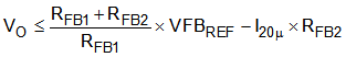
 Figure 7-15 OV and UV Faults
If the CHxOVFL bit is set to "1" in the FLATEN Register, the OV fault is configured as a latched fault and the associated channel turns off with the rising edge of CHx_OV. The channel can be turned on again only by re-setting the CHxEN bit in the EN Register.
For CHxOVFL = 0, the OV fault is a non-latched fault. In this case, the associated channel turns off when the OV fault occurs, but the channel goes through a restart and soft-start ramp when CHx_OV goes low. Figure 7-16 shows a non-latched OV situation for a converter in CV mode, where the output voltage (VFBx) is regulated to VFBREF in normal condition.
 Figure 7-16 Non-latched OV Fault in CV Mode