SLVSDF7A December 2016 – July 2017 TPSM84A21
PRODUCTION DATA.
- 1 Features
- 2 Applications
- 3 Description
- 4 Revision History
- 5 Pin Configuration and Functions
- 6 Specifications
-
7 Detailed Description
- 7.1 Overview
- 7.2 Functional Block Diagram
- 7.3
Feature Description
- 7.3.1 Adjusting the Output Voltage (VADJ)
- 7.3.2 Input and Output Capacitance
- 7.3.3 Transient Response
- 7.3.4 Oscillator Frequency
- 7.3.5 External Clock Syncronization
- 7.3.6 Soft Start
- 7.3.7 Power Good (PGOOD)
- 7.3.8 Gate Driver (VG)
- 7.3.9 Startup into Pre-biased Outputs
- 7.3.10 Thermal Shutdown
- 7.3.11 Overcurrent Protection
- 7.3.12 Output Undervoltage/Overvoltage Protection
- 7.3.13 Enable (EN)
- 7.3.14 Undervoltage Lockout (UVLO)
- 7.4 Device Functional Modes
- 8 Application and Implementation
- 9 Power Supply Recommendations
- 10Layout
- 11Device and Documentation Support
- 12Mechanical, Packaging, and Orderable Information
Package Options
Mechanical Data (Package|Pins)
- MOJ|20
Thermal pad, mechanical data (Package|Pins)
Orderable Information
10.3 EMI
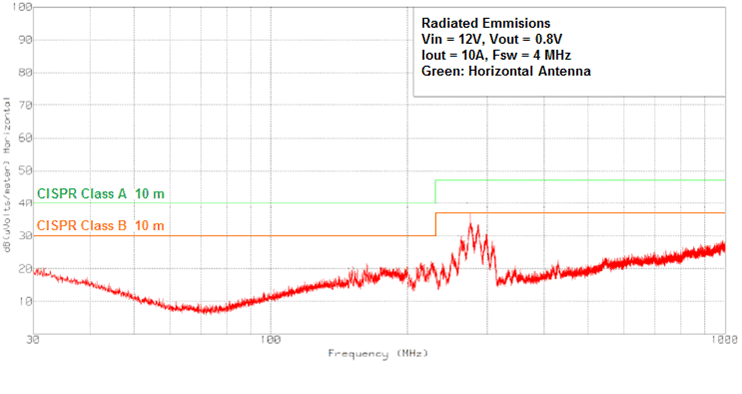
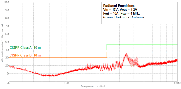
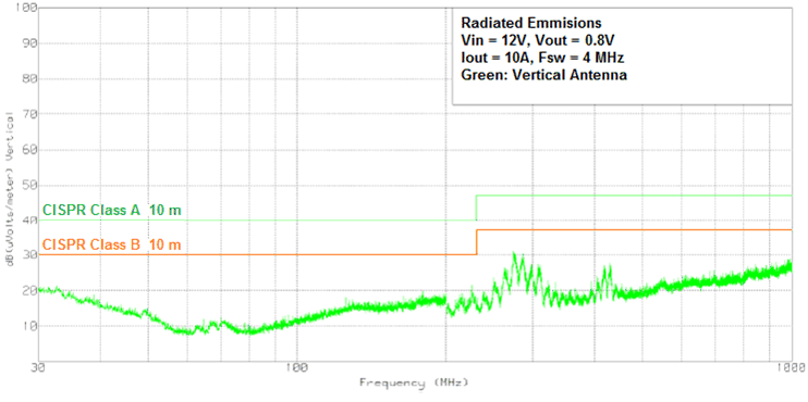
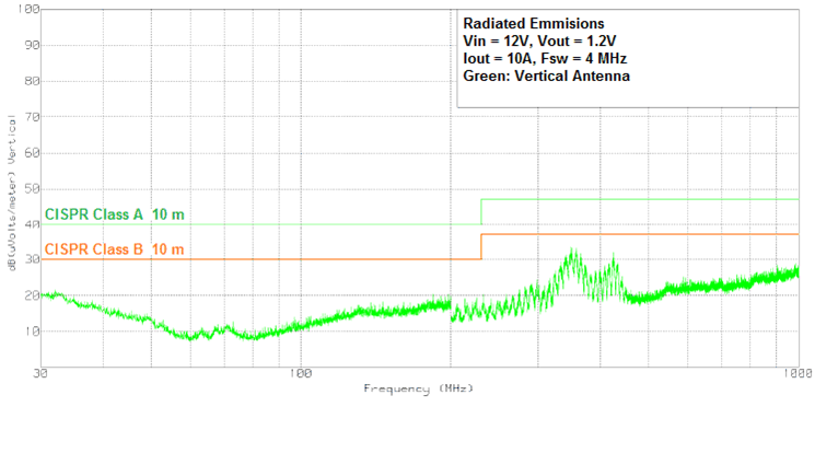
The TPSM84A21 is compliant with EN55022 Class B radiated emissions. Figure 24 to Figure 27 show typical examples of radiated emissions plots for the TPSM84A21. Graphs included show plots of the antenna in the horizontal and vertical positions.

10-A Load, Horizontal Antenna
 Figure 26. Radiated Emissions 12-V Input, 1.2-V Output,
10-A Load, Horizontal Antenna

10-A Load, Vertical Antenna
 Figure 27. Radiated Emissions 12-V Input, 1.2-V Output,
10-A Load, Vertical Antenna