SLVSDF7A December 2016 – July 2017 TPSM84A21
PRODUCTION DATA.
- 1 Features
- 2 Applications
- 3 Description
- 4 Revision History
- 5 Pin Configuration and Functions
- 6 Specifications
-
7 Detailed Description
- 7.1 Overview
- 7.2 Functional Block Diagram
- 7.3
Feature Description
- 7.3.1 Adjusting the Output Voltage (VADJ)
- 7.3.2 Input and Output Capacitance
- 7.3.3 Transient Response
- 7.3.4 Oscillator Frequency
- 7.3.5 External Clock Syncronization
- 7.3.6 Soft Start
- 7.3.7 Power Good (PGOOD)
- 7.3.8 Gate Driver (VG)
- 7.3.9 Startup into Pre-biased Outputs
- 7.3.10 Thermal Shutdown
- 7.3.11 Overcurrent Protection
- 7.3.12 Output Undervoltage/Overvoltage Protection
- 7.3.13 Enable (EN)
- 7.3.14 Undervoltage Lockout (UVLO)
- 7.4 Device Functional Modes
- 8 Application and Implementation
- 9 Power Supply Recommendations
- 10Layout
- 11Device and Documentation Support
- 12Mechanical, Packaging, and Orderable Information
Package Options
Mechanical Data (Package|Pins)
- MOJ|20
Thermal pad, mechanical data (Package|Pins)
Orderable Information
7.3.14 Undervoltage Lockout (UVLO)
The TPSM84A21 implements internal UVLO circuitry on the VIN pin. The device is disabled when the VIN pin voltage is below the internal VIN UVLO threshold. The internal VIN UVLO rising threshold is 7.65 V(max) with a typical hysteresis of 250 mV.
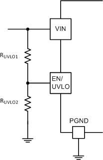
If an application requires a higher UVLO threshold, the UVLO pin can be configured as shown in Figure 16. The value of RUVLO1 and RUVLO2 can be calculated using Equation 3 and Equation 4 or selected from Table 2. It is recommended to set the UVLO hysteresis of approximately 500mV in order to avoid repeated chatter during start up or shut down. Table 2 shows recommended RUVLO1 and RUVLO2 values for various VIN UVLO rising thresholds, with 500 mV of hysteresis.


 Figure 16. Adjustable UVLO
 Table 2. Standard Resistor Values For Adjusting VIN UVLO
| VIN UVLO RISING THRESHOLD (V) | 8.0 | 8.5 | 9.0 | 9.5 | 10.0 |
|---|---|---|---|---|---|
| VIN UVLO FALLING THRESHOLD (V) | 7.5 | 8.0 | 8.5 | 9.0 | 9.5 |
| RUVLO1 (kΩ) | 169 | 169 | 169 | 169 | 169 |
| RUVLO2 (kΩ) | 29.4 | 27.4 | 25.5 | 24.3 | 22.6 |