SLWS223B August 2011 – November 2015 TRF3705
PRODUCTION DATA.
- 1 Features
- 2 Applications
- 3 Description
- 4 Revision History
- 5 Pin Configuration and Functions
-
6 Specifications
- 6.1 Absolute Maximum Ratings
- 6.2 ESD Ratings
- 6.3 Recommended Operating Conditions
- 6.4 Thermal Information
- 6.5 Electrical Characteristics: General
- 6.6 Electrical Characteristics
- 6.7 Typical Characteristics: Single-Tone Baseband
- 6.8 Typical Characteristics: Two-Tone Baseband
- 6.9 Typical Characteristics: Two-Tone Baseband, Mid-Band Calibration
- 6.10 Typical Characteristics: No Baseband
- 6.11 Typical Characteristics: Two-Tone Baseband
- 7 Detailed Description
- 8 Application and Implementation
- 9 Power Supply Recommendations
- 10Layout
- 11Device and Documentation Support
- 12Mechanical, Packaging, and Orderable Information
Package Options
Mechanical Data (Package|Pins)
- RGE|24
Thermal pad, mechanical data (Package|Pins)
- RGE|24
Orderable Information
1 Features
- High Linearity:
- Output IP3: 30 dBm at 1850 MHz
- Low Output Noise Floor: –160 dBm/Hz
- 78-dBc Single-Carrier WCDMA ACPR
at –10-dBm Channel Power - Unadjusted Carrier Suppression: –40 dBm
- Unadjusted Sideband Suppression: –45 dBc
- Single Supply: 3.3-V Operation
- 1-bit Gain Step Control
- Fast Power-Up/Power-Down
2 Applications
- Cellular Base Station Transmitter
- CDMA: IS95, UMTS, CDMA2000, TD-SCDMA
- LTE (Long Term Evolution)
- TDMA: GSM, EDGE/UWC-136
- Multicarrier GSM (MC-GSM)
- Wireless MAN Wideband Transceivers
3 Description
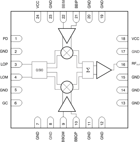
The TRF3705 is a low-noise direct quadrature modulator, capable of converting complex modulated signals from baseband or IF directly up to RF. The TRF3705 is a high-performance, superior-linearity device that is ideal to up-convert to RF frequencies of 300 MHz (Note: appropriate matching network is required for optimal performance at 300 MHz) through 4 GHz. The modulator is implemented as a double-balanced mixer.
The RF output block consists of a differential-to-single-ended converter that is capable of driving a single-ended 50-Ω load. The TRF3705 requires a 0.25-V common-mode voltage for optimum linearity performance. The TRF3705 also provides a fast power-down pin that can be used to reduce power dissipation in TDD applications.
The TRF3705 is available in an RGE-24 VQFN package.
Device Information(1)
| PART NUMBER | PACKAGE | BODY SIZE (NOM) |
|---|---|---|
| TRF3705 | VQFN (24) | 4.00 mm x 4.00 mm |
- For all available packages, see the orderable addendum at the end of the data sheet.
Block Diagram
