SLWS223B August 2011 – November 2015 TRF3705
PRODUCTION DATA.
- 1 Features
- 2 Applications
- 3 Description
- 4 Revision History
- 5 Pin Configuration and Functions
-
6 Specifications
- 6.1 Absolute Maximum Ratings
- 6.2 ESD Ratings
- 6.3 Recommended Operating Conditions
- 6.4 Thermal Information
- 6.5 Electrical Characteristics: General
- 6.6 Electrical Characteristics
- 6.7 Typical Characteristics: Single-Tone Baseband
- 6.8 Typical Characteristics: Two-Tone Baseband
- 6.9 Typical Characteristics: Two-Tone Baseband, Mid-Band Calibration
- 6.10 Typical Characteristics: No Baseband
- 6.11 Typical Characteristics: Two-Tone Baseband
- 7 Detailed Description
- 8 Application and Implementation
- 9 Power Supply Recommendations
- 10Layout
- 11Device and Documentation Support
- 12Mechanical, Packaging, and Orderable Information
Package Options
Mechanical Data (Package|Pins)
- RGE|24
Thermal pad, mechanical data (Package|Pins)
- RGE|24
Orderable Information
5 Pin Configuration and Functions
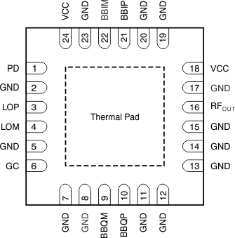
RGE Package
24 Pin VQFN
Top View

Pin Functions
| PIN | I/O | DESCRIPTION | |
|---|---|---|---|
| NO. | NAME | ||
| 1 | PD | I | Power-down digital input (high = device off) |
| 2 | GND | I | Ground |
| 3 | LOP | I | Local oscillator input |
| 4 | LOM | I | Local oscillator input |
| 5 | GND | I | Ground |
| 6 | GC | I | Gain control digital input (high = high gain) |
| 7 | GND | — | Ground or leave unconnected |
| 8 | GND | I | Ground |
| 9 | BBQM | I | In-quadrature input |
| 10 | BBQP | I | In-quadrature input |
| 11 | GND | I | Ground |
| 12 | GND | I | Ground |
| 13 | GND | I | Ground |
| 14 | GND | I | Ground |
| 15 | GND | I | Ground |
| 16 | RFOUT | O | RF output |
| 17 | GND | I | Ground |
| 18 | VCC | I | Power supply |
| 19 | GND | I | Ground |
| 20 | GND | I | Ground |
| 21 | BBIP | I | In-phase input |
| 22 | BBIM | I | In-phase input |
| 23 | GND | I | Ground |
| 24 | VCC | I | Power supply |