SLWS223B August 2011 – November 2015 TRF3705
PRODUCTION DATA.
- 1 Features
- 2 Applications
- 3 Description
- 4 Revision History
- 5 Pin Configuration and Functions
-
6 Specifications
- 6.1 Absolute Maximum Ratings
- 6.2 ESD Ratings
- 6.3 Recommended Operating Conditions
- 6.4 Thermal Information
- 6.5 Electrical Characteristics: General
- 6.6 Electrical Characteristics
- 6.7 Typical Characteristics: Single-Tone Baseband
- 6.8 Typical Characteristics: Two-Tone Baseband
- 6.9 Typical Characteristics: Two-Tone Baseband, Mid-Band Calibration
- 6.10 Typical Characteristics: No Baseband
- 6.11 Typical Characteristics: Two-Tone Baseband
- 7 Detailed Description
- 8 Application and Implementation
- 9 Power Supply Recommendations
- 10Layout
- 11Device and Documentation Support
- 12Mechanical, Packaging, and Orderable Information
Package Options
Mechanical Data (Package|Pins)
- RGE|24
Thermal pad, mechanical data (Package|Pins)
- RGE|24
Orderable Information
7 Detailed Description
7.1 Overview
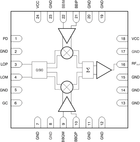
TRF3705 is a low-noise direct quadrature modulator with high linearity, capable of converting complex modulated signals from baseband or IF directly to RF. With high-performance and superior-linearity , TRF3705 is an ideal device to up-convert to RF frequencies of 300 MHz through 4 GHz. With appropriate matching network, optimal performance can be obtained. The modulator is implemented as a double-balanced mixer.
TRF3705 has a RF output block which consists of a differential-to-single-ended converter that is capable of directly driving a single-ended 50-Ω load. The TRF3705 requires a 0.25-V common-mode voltage for optimal linearity performance. With a fast power-down pin, TRF3705 can be used to reduce power dissipation in TDD application
7.2 Functional Block Diagram

7.3 Feature Description
7.3.1 Gain Control Feature
TRF3705 has a specific GC pin which is used for gain control. The GC pin is gain control digital input which is internally pulled down. When driving low or left open, modulator is in low gain mode. With driving high externally, the modulator is in high gain mode. This 1 bit gain step control feature offers a typical 3-dB gain increase in high gain mode. If power optimization is desired, driving this pin low can easily put the modulator into low gain mode.
7.4 Device Functional Modes
7.4.1 Power Down Mode
TRF3705 features a PD pin to power down the modulator. The PD pin is internally pulled down. When the power-down digital input pin is driven high, the device is off. This feature provides a fast power-down which can be used to reduce power dissipation in time division duplexing applications.