SLWS223B August 2011 – November 2015 TRF3705
PRODUCTION DATA.
- 1 Features
- 2 Applications
- 3 Description
- 4 Revision History
- 5 Pin Configuration and Functions
-
6 Specifications
- 6.1 Absolute Maximum Ratings
- 6.2 ESD Ratings
- 6.3 Recommended Operating Conditions
- 6.4 Thermal Information
- 6.5 Electrical Characteristics: General
- 6.6 Electrical Characteristics
- 6.7 Typical Characteristics: Single-Tone Baseband
- 6.8 Typical Characteristics: Two-Tone Baseband
- 6.9 Typical Characteristics: Two-Tone Baseband, Mid-Band Calibration
- 6.10 Typical Characteristics: No Baseband
- 6.11 Typical Characteristics: Two-Tone Baseband
- 7 Detailed Description
- 8 Application and Implementation
- 9 Power Supply Recommendations
- 10Layout
- 11Device and Documentation Support
- 12Mechanical, Packaging, and Orderable Information
Package Options
Mechanical Data (Package|Pins)
- RGE|24
Thermal pad, mechanical data (Package|Pins)
- RGE|24
Orderable Information
6 Specifications
6.1 Absolute Maximum Ratings(1)
Over operating free-air temperature range (unless otherwise noted).| MIN | MAX | UNIT | ||
|---|---|---|---|---|
| Supply voltage range(2) | –0.3 | 6 | V | |
| Digital I/O voltage range | –0.3 | VCC + 0.5 | V | |
| Operating virtual junction temperature range, TJ | –40 | 150 | °C | |
| Operating ambient temperature range, TA | –40 | 85 | °C | |
| Storage temperature range, Tstg | –65 | 150 | °C | |
(1) Stresses beyond those listed under absolute maximum ratings may cause permanent damage to the device. These are stress ratings only, and functional operation of the device at these or any other conditions beyond those indicated under recommended operating conditions is not implied. Exposure to absolute-maximum-rated conditions for extended periods may affect device reliability.
(2) All voltage values are with respect to network ground terminal.
6.2 ESD Ratings
| VALUE | UNIT | |||
|---|---|---|---|---|
| V(ESD) | Electrostatic discharge | Human-body model (HBM), per ANSI/ESDA/JEDEC JS-001(1) | ±4000 | V |
| Charged-device model (CDM), per JEDEC specification JESD22-C101(2) | ±250 | |||
(1) JEDEC document JEP155 states that 500-V HBM allows safe manufacturing with a standard ESD control process. .
(2) JEDEC document JEP157 states that 250-V CDM allows safe manufacturing with a standard ESD control process.
6.3 Recommended Operating Conditions
Over operating free-air temperature range (unless otherwise noted).| MIN | NOM | MAX | UNIT | ||
|---|---|---|---|---|---|
| VCC | Power-supply voltage | 3.15 | 3.3 | 3.6 | V |
6.4 Thermal Information
| THERMAL METRIC(1) | TRF3705 | UNIT | |
|---|---|---|---|
| RGE (VQFN) | |||
| 24 PINS | |||
| RθJA | Junction-to-ambient thermal resistance | 38.4 | °C/W |
| RθJC(top) | Junction-to-case (top) thermal resistance | 42.5 | °C/W |
| RθJB | Junction-to-board thermal resistance | 16.6 | °C/W |
| ψJT | Junction-to-top characterization parameter | 0.9 | °C/W |
| ψJB | Junction-to-board characterization parameter | 16.6 | °C/W |
| RθJC(bot) | Junction-to-case (bottom) thermal resistance | 6.6 | °C/W |
(1) For more information about traditional and new thermal metrics, see the Semiconductor and IC Package Thermal Metrics application report, SPRA953.
6.5 Electrical Characteristics: General
Over recommended operating conditions; at power supply = 3.3 V and TA = +25°C, unless otherwise noted.| PARAMETERS | TEST CONDITIONS | MIN | TYP | MAX | UNIT | |
|---|---|---|---|---|---|---|
| DC PARAMETERS | ||||||
| ICC | Total supply current | TA = +25°C, device on (PD = low) | 306 | mA | ||
| TA = +25°C, device off (PD = high) | 35 | μA | ||||
| LO INPUT | ||||||
| fLO | LO low frequency | 300 | MHz | |||
| LO high frequency | 4000 | MHz | ||||
| LO input power | –10 | 0 | +15 | dBm | ||
| BASEBAND INPUTS | ||||||
| VCM | I and Q input dc common-mode voltage | 0.25 | 0.5 | V | ||
| BW | 1-dB input frequency bandwidth | 1000 | MHz | |||
| ZI | Input impedance | Resistance | 8 | kΩ | ||
| Parallel capacitance | 4.6 | pF | ||||
| POWER ON/OFF | ||||||
| Turn on time | PD = low to 90% final output power | 0.2 | μs | |||
| Turn off time | PD = high to initial output power –30 dB | 0.2 | μs | |||
| DIGITAL INTERFACE | ||||||
| VIH | PD high-level input voltage | 2 | V | |||
| VIL | PD low-level input voltage | 0.8 | V | |||
6.6 Electrical Characteristics
Over recommended operating conditions; at power supply = 3.3 V, TA = +25°C, VCM = 0.25 V; LO Power = 0 dBm, single-ended (LOP); GC set low, VIN BB = 1.0 VPP (diff) in quadrature, and fBB = 5.5 MHz, standard broadband output matching circuit, unless otherwise noted.| PARAMETERS | TEST CONDITIONS | MIN | TYP | MAX | UNIT | |
|---|---|---|---|---|---|---|
| fLO = 400 MHz | ||||||
| G | Voltage gain | Output RMS voltage over input I (or Q) RMS voltage, GC set low | –4.7 | dB | ||
| Output RMS voltage over input I (or Q) RMS voltage, GC set high | –1.9 | dB | ||||
| POUT | Output power | GC set low | –0.7 | dBm | ||
| GC set high | 2.1 | dBm | ||||
| P1dB | Output compression point | GC set low | 8.5 | dBm | ||
| GC set high | 9.1 | dBm | ||||
| IP3 | Output IP3 | fBB1 = 4.5 MHz; fBB2 = 5.5 MHz; GC set low | 26 | dBm | ||
| fBB1 = 4.5 MHz; fBB2 = 5.5 MHz; GC set high | 25.4 | dBm | ||||
| IP2 | Output IP2 | Measured at fLO + (fBB1± fBB2), GC set low | 60.2 | dBm | ||
| Measured at fLO + (fBB1± fBB2), GC set high | 61.9 | dBm | ||||
| SBS | Unadjusted sideband suppression | –57.4 | dBc | |||
| CF | Unadjusted carrier feedthrough | Measured at LO frequency | –51.6 | dBm | ||
| Measured at 2 x LO | –50 | dBm | ||||
| Measured at 3 x LO | –49 | dBm | ||||
| Output noise floor | DC only to BB inputs; 10-MHz offset from LO | –166.7 | dBm/Hz | |||
| HD2BB | Baseband harmonics | Measured with ±1-MHz tone at 0.5 VPP each at fLO ±(2 x fBB) | –67 | dBc | ||
| HD3BB | Baseband harmonics | Measured with ±1-MHz tone at 0.5 VPP each at fLO ±(3 x fBB) | –64 | dBc | ||
| fLO = 750 MHz | ||||||
| G | Voltage gain | Output RMS voltage over input I (or Q) RMS voltage, GC set low | 0.2 | dB | ||
| Output RMS voltage over input I (or Q) RMS voltage, GC set high | 3.0 | dB | ||||
| POUT | Output power | GC set low | 4.2 | dBm | ||
| GC set high | 7 | dBm | ||||
| P1dB | Output compression point | GC set low | 13.3 | dBm | ||
| GC set high | 13.9 | dBm | ||||
| IP3 | Output IP3 | fBB1 = 4.5 MHz; fBB2 = 5.5 MHz; GC set low | 31.5 | dBm | ||
| fBB1 = 4.5 MHz; fBB2 = 5.5 MHz; GC set high | 30.8 | dBm | ||||
| IP2 | Output IP2 | Measured at fLO + (fBB1± fBB2), GC set low | 73.6 | dBm | ||
| Measured at fLO + (fBB1± fBB2), GC set high | 80.5 | dBm | ||||
| SBS | Unadjusted sideband suppression | –45.2 | dBc | |||
| CF | Unadjusted carrier feedthrough | Measured at LO frequency | –45.7 | dBm | ||
| Measured at 2 x LO | –46 | dBm | ||||
| Measured at 3 x LO | –53.5 | dBm | ||||
| Output noise floor | DC only to BB inputs; 10-MHz offset from LO | –159.9 | dBm/Hz | |||
| HD2BB | Baseband harmonics | Measured with ±1-MHz tone at 0.5 VPP each at fLO ±(2 x fBB) | –70 | dBc | ||
| HD3BB | Baseband harmonics | Measured with ±1-MHz tone at 0.5 VPP each at fLO ±(3 x fBB) | –66 | dBc | ||
| fLO = 900 MHz | ||||||
| G | Voltage gain | Output RMS voltage over input I (or Q) RMS voltage, GC set low | 0.3 | dB | ||
| Output RMS voltage over input I (or Q) RMS voltage, GC set high | 3.1 | dB | ||||
| POUT | Output power | GC set low | 4.3 | dBm | ||
| GC set high | 7.1 | dBm | ||||
| P1dB | Output compression point | GC set low | 13.2 | dBm | ||
| GC set high | 13.7 | dBm | ||||
| IP3 | Output IP3 | fBB1 = 4.5 MHz; fBB2 = 5.5 MHz; GC set low | 31.7 | dBm | ||
| fBB1 = 4.5 MHz; fBB2 = 5.5 MHz; GC set high | 30.9 | dBm | ||||
| IP2 | Output IP2 | Measured at fLO + (fBB1± fBB2), GC set low | 71.5 | dBm | ||
| Measured at fLO + (fBB1± fBB2), GC set high | 75.3 | dBm | ||||
| SBS | Unadjusted sideband suppression | –43.8 | dBc | |||
| CF | Unadjusted carrier feedthrough | Measured at LO frequency | –48.5 | dBm | ||
| Measured at 2 x LO | –53 | dBm | ||||
| Measured at 3 x LO | –50 | dBm | ||||
| Output noise floor | DC only to BB inputs; 10-MHz offset from LO | –157.9 | dBm/Hz | |||
| HD2BB | Baseband harmonics | Measured with ±1-MHz tone at 0.5 VPP each at fLO ±(2 x fBB) | –80 | dBc | ||
| HD3BB | Baseband harmonics | Measured with ±1-MHz tone at 0.5 VPP each at fLO ±(3 x fBB) | –65 | dBc | ||
| fLO = 1840 MHz | ||||||
| G | Voltage gain | Output RMS voltage over input I (or Q) RMS voltage, GC set low | –0.1 | dB | ||
| Output RMS voltage over input I (or Q) RMS voltage, GC set high | 2.5 | dB | ||||
| POUT | Output power | GC set low | 3.9 | dBm | ||
| GC set high | 6.5 | dBm | ||||
| P1dB | Output compression point | GC set low | 13.2 | dBm | ||
| GC set high | 13.6 | dBm | ||||
| IP3 | Output IP3 | fBB1 = 4.5 MHz; fBB2 = 5.5 MHz; GC set low | 32.1 | dBm | ||
| fBB1 = 4.5 MHz; fBB2 = 5.5 MHz; GC set high | 30.3 | dBm | ||||
| IP2 | Output IP2 | Measured at fLO + (fBB1± fBB2), GC set low | 60.8 | dBm | ||
| Measured at fLO + (fBB1± fBB2), GC set high | 62 | dBm | ||||
| SBS | Unadjusted sideband suppression | –43.4 | dBc | |||
| CF | Unadjusted carrier feedthrough | Measured at LO frequency | –42.4 | dBm | ||
| Measured at 2 x LO | –41 | dBm | ||||
| Measured at 3 x LO | –53 | dBm | ||||
| Output noise floor | DC only to BB inputs; 10-MHz offset from LO | –158.8 | dBm/Hz | |||
| HD2BB | Baseband harmonics | Measured with ±1-MHz tone at 0.5 VPP each at fLO ±(2 x fBB) | –69 | dBc | ||
| HD3BB | Baseband harmonics | Measured with ±1-MHz tone at 0.5 VPP each at fLO ±(3 x fBB) | –80 | dBc | ||
| fLO = 2140 MHz | ||||||
| G | Voltage gain | Output RMS voltage over input I (or Q) RMS voltage, GC set low | 0.1 | dB | ||
| Output RMS voltage over input I (or Q) RMS voltage, GC set high | 2.9 | dB | ||||
| POUT | Output power | GC set low | 4.1 | dBm | ||
| GC set high | 6.9 | dBm | ||||
| P1dB | Output compression point | GC set low | 13.1 | dBm | ||
| GC set high | 13.5 | dBm | ||||
| IP3 | Output IP3 | fBB1 = 4.5 MHz; fBB2 = 5.5 MHz; GC set low | 28.6 | dBm | ||
| fBB1 = 4.5 MHz; fBB2 = 5.5 MHz; GC set high | 27.6 | dBm | ||||
| IP2 | Output IP2 | Measured at fLO + (fBB1± fBB2), GC set low | 65.5 | dBm | ||
| Measured at fLO + (fBB1± fBB2), GC set high | 68.2 | dBm | ||||
| SBS | Unadjusted sideband suppression | –45.6 | dBc | |||
| CF | Unadjusted carrier feedthrough | Measured at LO frequency | –39.3 | dBm | ||
| Measured at 2 x LO | –37 | dBm | ||||
| Measured at 3 x LO | –46 | dBm | ||||
| Output noise floor | DC only to BB inputs; 10-MHz offset from LO | –160.0 | dBm/Hz | |||
| HD2BB | Baseband harmonics | Measured with ±1-MHz tone at 0.5 VPP each at fLO ±(2 x fBB) | –61 | dBc | ||
| HD3BB | Baseband harmonics | Measured with ±1-MHz tone at 0.5 VPP each at fLO ±(3 x fBB) | –60 | dBc | ||
| fLO = 2600 MHz | ||||||
| G | Voltage gain | Output RMS voltage over input I (or Q) RMS voltage, GC set low | –0.8 | dB | ||
| Output RMS voltage over input I (or Q) RMS voltage, GC set high | 2 | dB | ||||
| POUT | Output power | GC set low | 3.2 | dBm | ||
| GC set high | 5.6 | dBm | ||||
| P1dB | Output compression point | GC set low | 12.5 | dBm | ||
| GC set high | 12.8 | dBm | ||||
| IP3 | Output IP3 | fBB1 = 4.5 MHz; fBB2 = 5.5 MHz; GC set low | 28 | dBm | ||
| FfBB1 = 4.5 MHz; fBB2 = 5.5 MHz; GC set high | 27.2 | dBm | ||||
| IP2 | Output IP2 | Measured at fLO + (fBB1± fBB2), GC set low | 67.9 | dBm | ||
| Measured at fLO + (fBB1± fBB2), GC set high | 66.4 | dBm | ||||
| SBS | Unadjusted sideband suppression | –52.9 | dBm | |||
| CF | Unadjusted carrier feedthrough | Measured at LO frequency | –37.8 | dBm | ||
| Measured at 2 x LO | –41 | dBm | ||||
| Measured at 3 x LO | –42 | dBm | ||||
| Output noise floor | DC only to BB inputs; 10-MHz offset from LO | –160.6 | dBm/Hz | |||
| HD2BB | Baseband harmonics | Measured with ±1-MHz tone at 0.5 VPP each at fLO ±(2 x fBB) | –67 | dBc | ||
| HD3BB | Baseband harmonics | Measured with ±1-MHz tone at 0.5 VPP each at fLO ±(3 x fBB) | –59 | dBc | ||
| fLO = 3500 MHz | ||||||
| G | Voltage gain | Output RMS voltage over input I (or Q) RMS voltage, GC set low | –1 | dB | ||
| Output RMS voltage over input I (or Q) RMS voltage, GC set high | 1.8 | dB | ||||
| POUT | Output power | GC set low | 3 | dBm | ||
| GC set high | 5.8 | dBm | ||||
| P1dB | Output compression point | GC set low | 12.1 | dBm | ||
| GC set high | 12.3 | dBm | ||||
| IP3 | Output IP3 | fBB1 = 4.5 MHz; fBB2 = 5.5 MHz; GC set low | 23.8 | dBm | ||
| fBB1 = 4.5 MHz; fBB2 = 5.5 MHz; GC set high | 25.3 | dBm | ||||
| IP2 | Output IP2 | Measured at fLO + (fBB1± fBB2), GC set low | 47.8 | dBm | ||
| Measured at fLO + (fBB1± fBB2), GC set high | 48.6 | dBm | ||||
| SBS | Unadjusted sideband suppression | –45.2 | dBm | |||
| CF | Unadjusted carrier feedthrough | Measured at LO frequency | –31.6 | dBm | ||
| Measured at 2 x LO | –30 | dBm | ||||
| Measured at 3 x LO | –53 | dBm | ||||
| Output noise floor | DC only to BB inputs; 10-MHz offset from LO | –160.6 | dBm/Hz | |||
| HD2BB | Baseband harmonics | Measured with ±1-MHz tone at 0.5 VPP each at fLO ±(2 x fBB) | –54 | dBc | ||
| HD3BB | Baseband harmonics | Measured with ±1-MHz tone at 0.5 VPP each at fLO ±(3 x fBB) | –50 | dBc | ||
6.7 Typical Characteristics: Single-Tone Baseband
VCC = 3.3 V; TA = 25°C; LO = 0 dBm, single-ended drive (LOP); I/Q frequency (fBB) = 5.5 MHz; baseband I/Q amplitude = 1-VPP differential sine waves in quadrature with VCM = 0.25 V; and broadband output match, unless otherwise noted.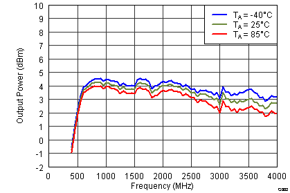 Figure 1. Output Power vs LO Frequency (fLO) and Temperature
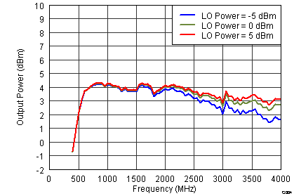 Figure 3. Output Power vs LO Frequency (fLO) Over LO Drive Level
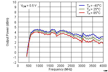 Figure 5. Output Power vs LO Frequency (fLO) and Temperature at VCM = 0.5 V
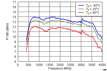 Figure 7. P1dB vs LO Frequency (fLO) and Temperature
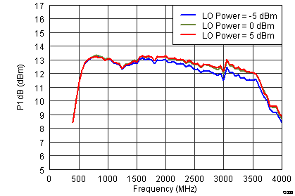 Figure 9. P1dB vs LO Frequency (fLO) and LO Drive Level
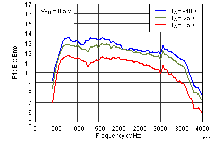 Figure 11. P1dB vs LO Frequency (fLO) and Temperature AT VCM = 0.5 V
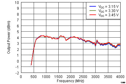 Figure 2. Output Power vs LO Frequency (fLO) and Supply Voltage
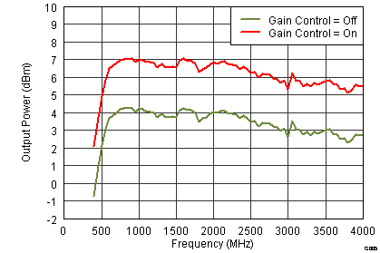 Figure 4. Output Power vs LO Frequency (fLO) and Gain Select Setting
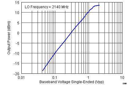 Figure 6. Output Power vs Baseband Voltage at 2140 MHz
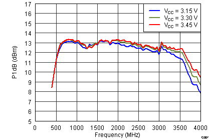 Figure 8. P1dB vs LO Frequency (fLO) and Supply Voltage
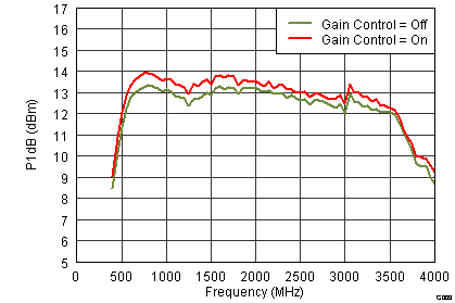 Figure 10. P1dB vs LO Frequency (fLO) and Gain Select Setting
6.8 Typical Characteristics: Two-Tone Baseband
VCC = 3.3 V; TA = 25°C; LO = 0 dBm, single-ended drive (LOP); I/Q frequency (fBB) = 4.5 MHz, 5.5 MHz; baseband I/Q amplitude = 0.5-VPP/tone differential sine waves in quadrature with VCM = 0.25 V; and broadband output match, unless otherwise noted.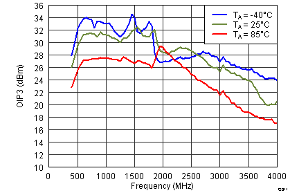 Figure 12. OIP3 vs LO Frequency (fLO) and Temperature
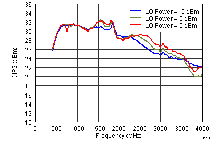 Figure 14. OIP3 vs LO Frequency (fLO) and LO Drive Level
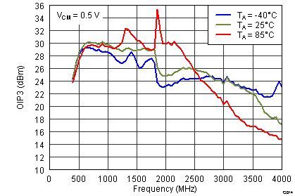 Figure 16. OIP3 vs LO Frequency (fLO) and Temperature AT VCM = 0.5 V
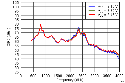 Figure 18. OIP2 vs LO Frequency (fLO) and Supply Voltage
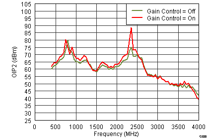 Figure 20. OIP2 vs LO Frequency (fLO) and Gain Select Setting
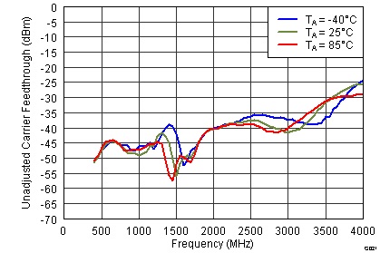 Figure 22. Unadjusted Carrier Feedthrough vs LO Frequency (fLO) and Temperature
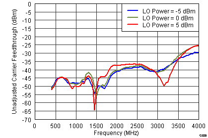 Figure 24. Unadjusted Carrier Feedthrough vs LO Frequency (fLO) and LO Drive Level
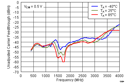 Figure 26. Unadjusted Carrier Feedthrough vs LO Frequency (fLO) and Temperature at VCM = 0.5 V
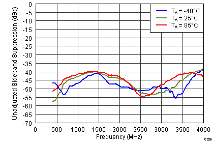 Figure 28. Unadjusted Sideband Suppression vs LO Frequency (fLO) and Temperature
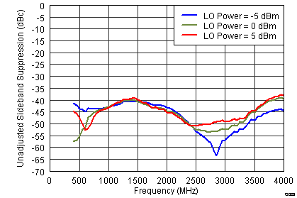 Figure 30. Unadjusted Sideband Suppression vs LO Frequency (fLO) and LO Drive Level
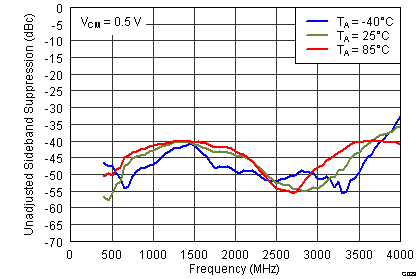 Figure 32. Unadjusted sideband Suppression vs LO Frequency (fLO) and Temperature at VCM = 0.5 V
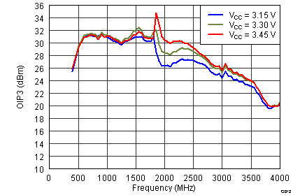 Figure 13. OIP3 vs LO FRequency (fLO) anD Supply Voltage
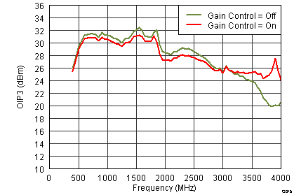 Figure 15. OIP3 vs LO Frequency (fLO) And Gain Select Setting
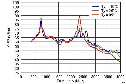 Figure 17. OIP2 vs LO Frequency (fLO) and Temperature
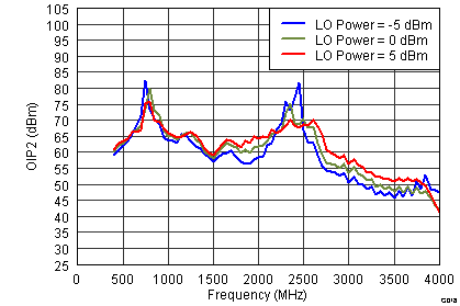 Figure 19. OIP2 vs LO Frequency (fLO) and LO Drive Level
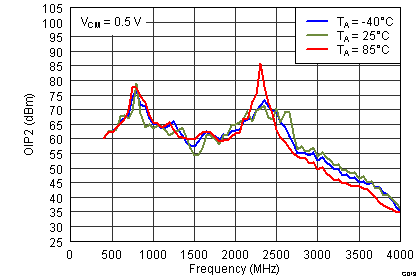 Figure 21. OIP2 vs LO Frequency (fLO) and Temperature AT VCM = 0.5 V
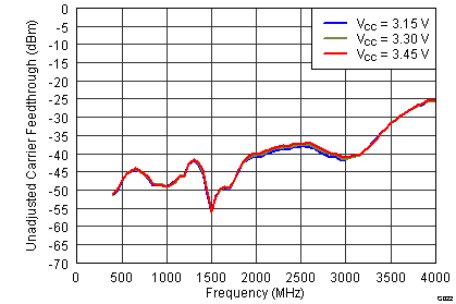 Figure 23. Unadjusted Carrier Feedthrough vs LO Frequency (fLO) and Supply Voltage
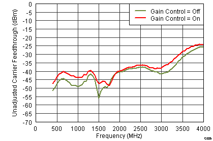 Figure 25. Unadjusted Carrier Feedthrough vs LO Frequency (fLO) and Gain Select Setting
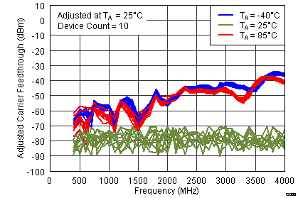 Figure 27. Carrier Feedthrough vs LO Frequency (fLO) and Temperature After Nulling at 25°C; Multiple Devices
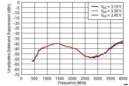 Figure 29. Unadjusted Sideband Suppression vs LO Frequency (fLO) and Supply Voltage
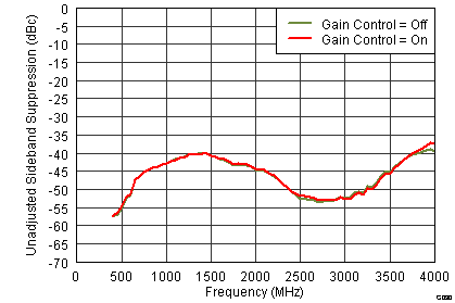 Figure 31. Unadjusted Sideband Suppression vs LO Frequency (fLO) and Gain Select Setting
6.9 Typical Characteristics: Two-Tone Baseband, Mid-Band Calibration
VCC = 3.3 V; TA = 25°C; LO = 0 dBm, single-ended drive (LOP); I/Q frequency (fBB) = 4.5 MHz, 5.5 MHz; baseband I/Q amplitude = 0.5-VPP/tone differential sine waves in quadrature with VCM = 0.25 V; and broadband output match, unless otherwise noted. Single point adjustment mid-band. Figure 33. Adjusted Carrier Feedthrough vs LO Frequency and Temperature (750 LTE Band)
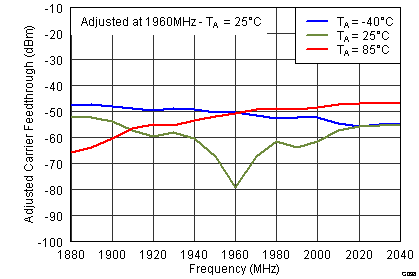 Figure 35. Adjusted Carrier Feedthrough vs LO Frequency and Temperature (PCS Band)
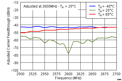 Figure 37. Adjusted Carrier Feedthrough vs LO Frequency and Temperature (2.6 GHz LTE Band)
 Figure 39. Adjusted Sideband Suppression vs LO Frequency and Temperature (750 LTE Band)
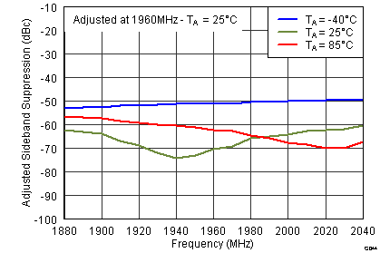 Figure 41. Adjusted Sideband Suppression vs LO Frequency and Temperature (PCS Band)
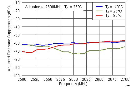 Figure 43. Adjusted Sideband Suppression vs LO Frequency and Temperature (2.6 GHz LTE Band)
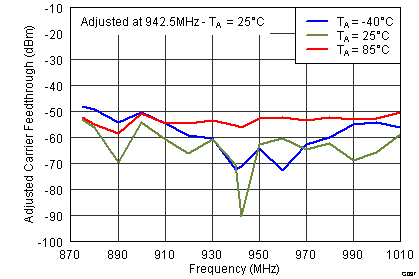 Figure 34. Adjusted Carrier Feedthrough vs LO Frequency and Temperature (GSM900 Band)
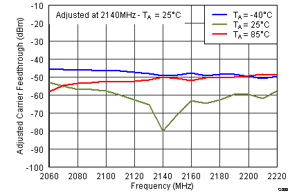 Figure 36. Adjusted carrier Feedthrough vs LO Frequency and Temperature (UMTS Band)
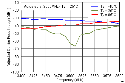 Figure 38. Adjusted Carrier Feedthrough vs LO Frequency and Temperature (WiMAX/LTE Band)
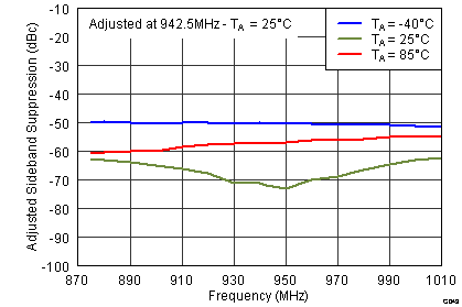 Figure 40. Adjusted Sideband Suppression vs LO Frequency and Temperature (GSM900 Band)
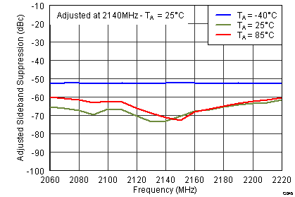 Figure 42. Adjusted Sideband Suppression vs LO Frequency and Temperature (UMTS Band)
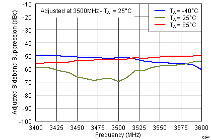 Figure 44. Adjusted Sideband Suppression vs LO Frequency and Temperature (WiMAX/LTE Band)
6.10 Typical Characteristics: No Baseband
VCC = 3.3 V; TA = 25°C; LO = 0 dBm, single-ended drive (LOP); and input baseband ports terminated in 50 Ω, unless otherwise noted.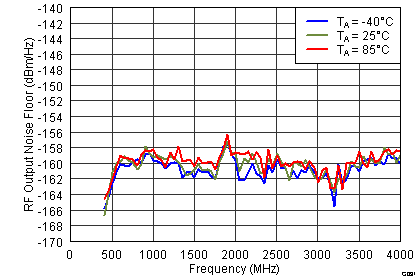 Figure 45. Output noisE vs LO Frequency (fLO) and Temperature
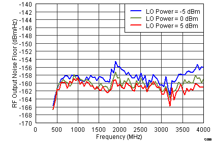 Figure 47. Output Noise vs LO Frequency (fLO) AND LO Drive Level
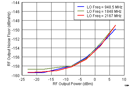 Figure 49. Output Noise vs Output Power
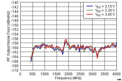 Figure 46. Output Noise vs LO Frequency (fLO) and Supply Voltage
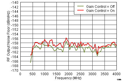 Figure 48. OUtput Noise vs LO Frequency (fLO) and Gain Select Setting
6.11 Typical Characteristics: Two-Tone Baseband
VCC = 3.3 V; TA = 25°C; LO = 0 dBm, single-ended drive (LOP); I/Q frequency (fBB) = 4.5 MHz, 5.5 MHz; baseband I/Q amplitude = 0.5-VPP/tone differential sine waves in quadrature with VCM = 0.25 V; and broadband output match, unless otherwise noted.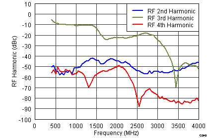 Figure 50. RF Harmonics vs LO FRequency (fLO)
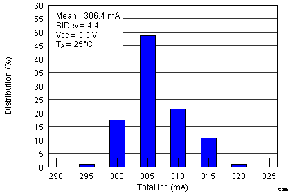 Figure 52. Nominal Current Consumption Distribution
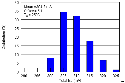 Figure 54. Current Consumption Distribution Over VCC
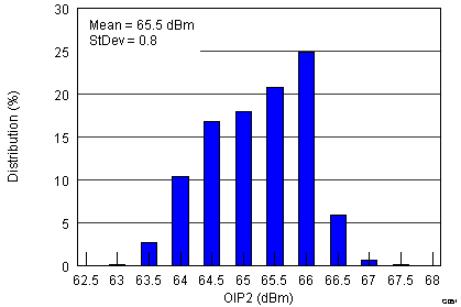 Figure 56. OIP2 Distribution at fLO = 2140 MHz
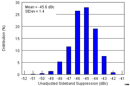 Figure 58. Unadjusted Sideband Suppression DIstribution at fLO = 2140 MHz
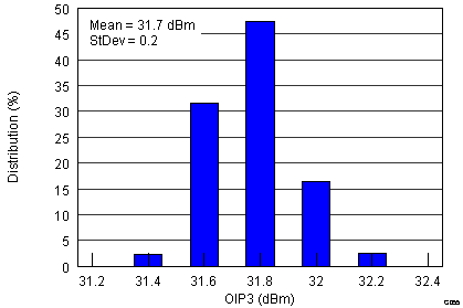 Figure 60. OIP3 Distribution at fLO = 900 MHz
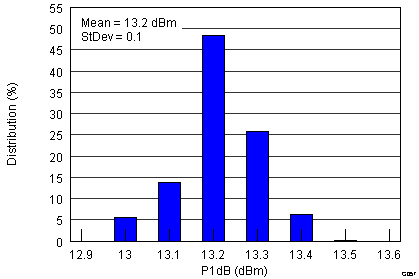 Figure 62. P1dB distribution at fLO = 900 MHz, fBB = 5.5 MHz
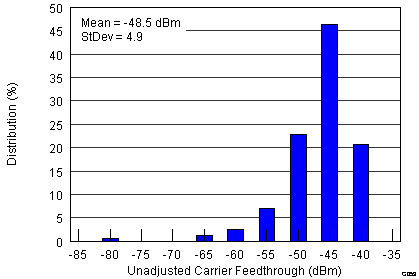 Figure 64. Unadjusted Carrier Feedthrough Distribution at fLO = 900 MHz
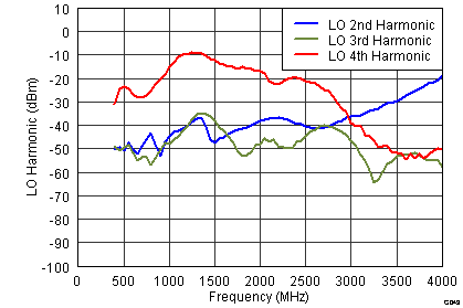 Figure 51. LO Harmonics vs LO Frequency (fLO)
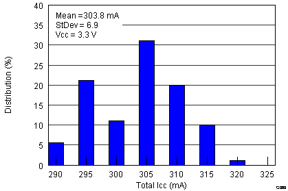 Figure 53. Current Consumption Distribution Over Temperature
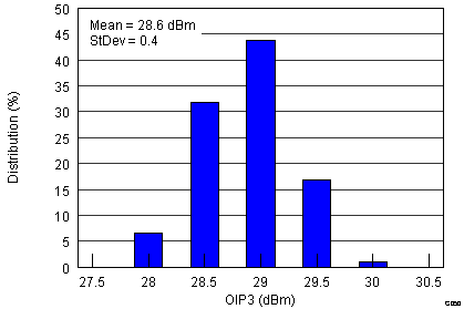 Figure 55. OIP3 Distribution at fLO = 2140 MHz
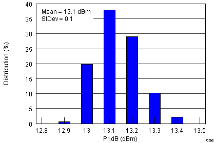 Figure 57. P1dB Distribution at fLO = 2140 MHz, fBB = 5.5 MHz
 Figure 59. Unadjusted Carrier Feedthrough Distribution at fLO = 2140 MHz
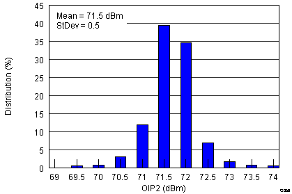 Figure 61. OIP2 Distribution at fLO = 900 MHz
 Figure 63. Unadjusted Sideband Suppression Distribution at fLO = 900 MHz