SLWS223B August 2011 – November 2015 TRF3705
PRODUCTION DATA.
- 1 Features
- 2 Applications
- 3 Description
- 4 Revision History
- 5 Pin Configuration and Functions
-
6 Specifications
- 6.1 Absolute Maximum Ratings
- 6.2 ESD Ratings
- 6.3 Recommended Operating Conditions
- 6.4 Thermal Information
- 6.5 Electrical Characteristics: General
- 6.6 Electrical Characteristics
- 6.7 Typical Characteristics: Single-Tone Baseband
- 6.8 Typical Characteristics: Two-Tone Baseband
- 6.9 Typical Characteristics: Two-Tone Baseband, Mid-Band Calibration
- 6.10 Typical Characteristics: No Baseband
- 6.11 Typical Characteristics: Two-Tone Baseband
- 7 Detailed Description
- 8 Application and Implementation
- 9 Power Supply Recommendations
- 10Layout
- 11Device and Documentation Support
- 12Mechanical, Packaging, and Orderable Information
Package Options
Mechanical Data (Package|Pins)
- RGE|24
Thermal pad, mechanical data (Package|Pins)
- RGE|24
Orderable Information
8 Application and Implementation
NOTE
Information in the following applications sections is not part of the TI component specification, and TI does not warrant its accuracy or completeness. TI’s customers are responsible for determining suitability of components for their purposes. Customers should validate and test their design implementation to confirm system functionality.
8.1 Application Information
TRF3705 is a quadrature modulator for up-converting the in-phase (I) and the quadrature-phase (Q) signals to radio frequency (RF) in the transmit chain. Typically, the device is used between the digital-to-analog converter (DAC) and the RF power amplifier.
8.2 Typical Application
8.2.1 Design Requirements
For this design example, use the parameters shown in Table 1.
Table 1. Pin Termination Requirements and Limitations
| NAME | PIN NO | DESCRIPTION |
|---|---|---|
| BBQM | 9 | Base-band in-quadrature input: negative terminal. Input impedance is 8 KΩ//4.6 pF. Optimal linearity is obtained if VCM is 0.25 V. Normally terminated in 50 Ω |
| BBQP | 10 | Base-band in-quadrature input: positive terminal. Input impedance is 8 KΩ//4.6 pF. Optimal linearity is obtained if VCM is 0.25 V. Normally terminated in 50 Ω |
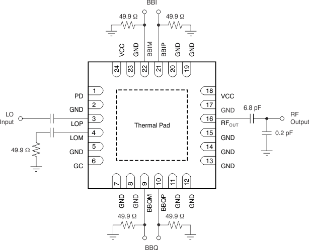
| LOP | 3 | Local oscillator input: positive terminal. This is preferred port when driving single ended. Normally AC coupled and terminated in 50 Ω |
| LOM | 4 | Local oscillator input: negative terminal. When driving LO single-ended, normally AC coupled and terminated in 50 Ω. |
| RFOUT | 16 | RF output. Normally using optimal matching circuits to match RF output to 50 Ω. Normally AC coupled. |
| GC | 6 | Gain control digital input. Internally pulled down. When driving high, get 3 dB gain increase of RF output. |
| PD | 1 | Power down digital input. Internally pulled down. When driving high, the modulator is off. |
| VCC | 18,24 | 3.3-V power supply. Can be tied together and source from a single clean supply. Each pin should be properly RF bypassed and decoupled. |
8.2.2 Detailed Design Procedure
8.2.2.1 Baseband Inputs
The baseband inputs consist of the in-phase signal (I) and the Quadrature-phase signal (Q). The I and Q lines are differential lines that are driven in quadrature. The nominal drive level is 1-VPP differential on each branch.
The baseband lines are nominally biased at 0.25-V common-mode voltage (VCM); however, the device can operate with a VCM in the range of 0 V to 0.5 V. The baseband input lines are normally terminated in 50 Ω, though it is possible to modify this value if necessary to match to an external filter load impedance requirement.
8.2.2.2 LO Input
The LO inputs can be driven either single-ended or differentially. There is no significant performance difference between either option with the exception of the sideband suppression. If driven single-ended, either input can be used, but LOP (pin 3) is recommended for best broadband performance of sideband suppression. When driving in single-ended configuration, simply ac-couple the unused port and terminate in 50 Ω. The comparison of the sideband suppression performance is shown in Figure 71 for driving the LO single-ended from either pin and for driving the LO input differentially.
8.2.2.3 RF Output
The RF output must be ac-coupled and can drive a 50-Ω load. The suggested output match provides the best broadband performance across the frequency range of the device. It is possible to modify the output match to optimize performance within a selected band if needed. The optimized matching circuits are to match the RF output impedances to 50 Ω.
Figure 72 shows a slightly better OIP3 performance at the frequency above 1850 MHz with an 0.2-pF matching capacitor.
8.2.2.4 350-MHz Operation
A different matching circuit, as shown in Figure 66, could also be applied to improve the performance for the frequency from 300 MHz to 400 MHz.
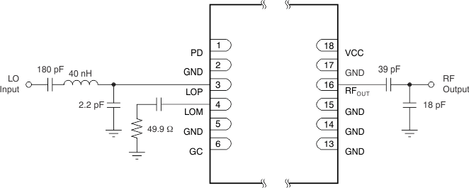 Figure 66. Matching Components for Operation Centered at 350 MHz
Figure 73 and Figure 74 show a slight improvement in OIP3 performance at frequencies above 1850 MHz with an 0.2-pF matching capacitor.
8.2.2.5 DAC to Modulator Interface Network
For optimum linearity and dynamic range, a digital-to-analog converter (DAC) can interface directly with the TRF3705 modulator. It is imperative that the common-mode voltage of the DAC and the modulator baseband inputs be properly maintained. With the proper interface network, the common-mode voltage of the DAC can be translated to the proper common-mode voltage of the modulator. The TRF3705 common-mode voltage is typically 0.25 V, and is ideally suited to interface with the DAC3482/3484 (DAC348x) family because the common-mode voltages of both devices are the same; there is no translation network required. The interface network is shown in Figure 67.
 Figure 67. DAC348x Interface with the TRF3705 Modulator
The DAC348x requires a load resistor of 25 Ω per branch to maintain its optimum voltage swing of 1-VPP differential with a 20-mA max current setting. The load of the DAC is separated into two parallel 50-Ω resistors placed on the input and output side of the low-pass filter. This configuration provides the proper resistive load to the DAC while also providing a convenient 50-Ω source and load termination for the filter.
8.2.2.6 DAC348x with TRF3705 Modulator Performance
The combination of the DAC348x driving the TRF3705 modulator yields excellent system parameters suitable for high-performance applications. As an example, the following sections illustrate the typical modulated adjacent channel power ratio (ACPR) for common telecom standards and bands. These measurements were taken on the DAC348x evaluation board.
8.2.2.6.1 WCDMA
The adjacent channel power ratio (ACPR) performance using a single-carrier WCDMA signal in the UMTS band is shown in Figure 68.
 Figure 68. Single-Carrier WCDMA ACPR, IF = 30 MHz, LO Frequency = 2110 MHz
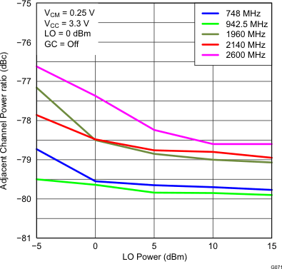
A marginal improvement in OIP3 and output noise performance can be observed by increasing the LO drive power, resulting in slightly improved ACPR performance. The ACPR performance versus LO drive level is plotted in Figure 75 across common frequencies to illustrate the amount of improvement that is possible.
8.2.2.6.2 LTE
ACPR performance using a 10 MHz LTE signal in the 700-MHz band is shown in Figure 69.
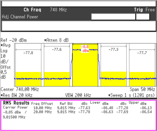 Figure 69. 10 MHz LTE ACPR, IF = 30 MHz, LO Frequency = 718 MHz
8.2.2.6.3 MC-GSM
ACPR performance using a four-carrier MC-GSM signal in the 1800-MHz band is shown in Figure 70.
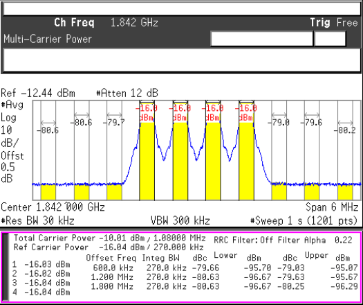 Figure 70. Four-Carrier MC-GSM, IF = 30 MHz ACPR, LO Frequency = 1812 MHz
8.2.3 Application Curves
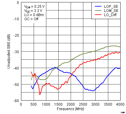 Figure 71. Unadjusted Sideband Suppression (SBS) vs LO Drive Options
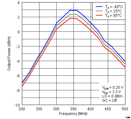 Figure 73. Output Power with 350-MHz Matching Circuit
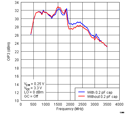 Figure 72. OIP3 with and without a Shunt 0.2-pF Matching Capacitor at the RF Port
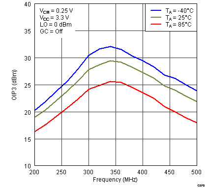 Figure 74. OIP3 with 350-MHz Matching Circuit
