SLWS223B August 2011 – November 2015 TRF3705
PRODUCTION DATA.
- 1 Features
- 2 Applications
- 3 Description
- 4 Revision History
- 5 Pin Configuration and Functions
-
6 Specifications
- 6.1 Absolute Maximum Ratings
- 6.2 ESD Ratings
- 6.3 Recommended Operating Conditions
- 6.4 Thermal Information
- 6.5 Electrical Characteristics: General
- 6.6 Electrical Characteristics
- 6.7 Typical Characteristics: Single-Tone Baseband
- 6.8 Typical Characteristics: Two-Tone Baseband
- 6.9 Typical Characteristics: Two-Tone Baseband, Mid-Band Calibration
- 6.10 Typical Characteristics: No Baseband
- 6.11 Typical Characteristics: Two-Tone Baseband
- 7 Detailed Description
- 8 Application and Implementation
- 9 Power Supply Recommendations
- 10Layout
- 11Device and Documentation Support
- 12Mechanical, Packaging, and Orderable Information
Package Options
Mechanical Data (Package|Pins)
- RGE|24
Thermal pad, mechanical data (Package|Pins)
- RGE|24
Orderable Information
11 Device and Documentation Support
11.1 Device Support
11.1.1 Definition of Specifications
11.1.1.1 Carrier Feedthrough
This specification measures the power of the local oscillator component that is present at the output spectrum of the modulator. The performance depends on the dc offset balance within the baseband input lines. Ideally, if all of the baseband lines were perfectly matched, the carrier (that is, the LO) would be naturally suppressed; however, small dc offset imbalances within the device allow some of the LO component to feed through to the output. This parameter is expressed as an absolute power in dBm, and is independent of the RF output power and the injected LO input power.
It is possible to adjust the baseband dc offset balance to suppress the output carrier component. Devices such as the DAC348x DAC family have dc offset adjustment capabilities specifically for this function. The Adjusted Carrier Feedthrough graphs (see Figure 33 through Figure 38) optimize the performance at the center of the band at room temperature. Then, with the adjusted dc offset values held constant, the parameter is measured over the frequency band and across the temperature extremes. The typical performance plots provide an indication of how well the adjusted carrier suppression can be maintained over frequency and temperature with only one calibration point.
11.1.1.2 Sideband Suppression
This specification measures the suppression of the undesired sideband at the output of the modulator relative to the desired sideband. If the amplitude and phase within the I and Q branch of the modulator were perfectly matched, the undesired sideband (or image) would be naturally suppressed. Amplitude and phase imbalance in the I and Q branches result in the increase of the undesired sideband. This parameter is measured in dBc relative to the desired sideband.
It is possible to adjust the relative amplitude and phase balance within the baseband lines to suppress the unwanted sideband. Devices such as the DAC348x DAC family have amplitude and phase adjustment control specifically for this function. The Adjusted Sideband Suppression graphs (refer to Figure 39 through Figure 44) optimize the performance at the center of the band at room temperature. Then, with the adjusted amplitude and phase values held constant, the parameter is measured over the frequency band and across the temperature extremes. The performance plots provide an indication of how well the adjusted sideband suppression can be maintained over frequency and temperature with only one calibration point.
11.1.1.3 Output Noise
The output noise specifies the absolute noise power density that is output from the RFOUT pin (pin 16). This parameter is expressed in dBm/Hz. This parameter, in conjunction with the OIP3 specification, indicates the dynamic range of the device. In general, at high output signal levels the performance is limited by the linearity of the device; at low output levels, on the other hand, the performance is limited by noise. As a result of the higher gain and output power of the TRF3705 compared to earlier devices, it is expected that the noise density is slightly higher as well. With its increased gain and high OIP3 performance, the overall dynamic range of the TRF3705 is maintained at exceptional levels.
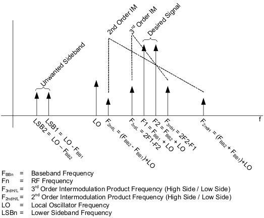
11.1.1.4 Definition of Terms
A simulated output spectrum with two tones is shown in Figure 77, with definitions of various terms used in this data sheet.
11.2 Community Resources
The following links connect to TI community resources. Linked contents are provided "AS IS" by the respective contributors. They do not constitute TI specifications and do not necessarily reflect TI's views; see TI's Terms of Use.
-
TI E2E™ Online Community TI's Engineer-to-Engineer (E2E) Community. Created to foster collaboration among engineers. At e2e.ti.com, you can ask questions, share knowledge, explore ideas and help solve problems with fellow engineers.
-
Design Support TI's Design Support Quickly find helpful E2E forums along with design support tools and contact information for technical support.
11.3 Trademarks
PowerPAD, E2E are trademarks of Texas Instruments.
All other trademarks are the property of their respective owners.
11.4 Glossary
SLYZ022 — TI Glossary.
This glossary lists and explains terms, acronyms, and definitions.
