SCDS228F AUGUST 2006 – December 2015 TS3A4741 , TS3A4742
UNLESS OTHERWISE NOTED, this document contains PRODUCTION DATA.
- 1 Features
- 2 Applications
- 3 Description
- 4 Revision History
- 5 Pin Configuration and Functions
- 6 Specifications
- 7 Parameter Measurement Information
- 8 Detailed Description
- 9 Application and Implementation
- 10Power Supply Recommendations
- 11Layout
- 12Device and Documentation Support
- 13Mechanical, Packaging, and Orderable Information
Package Options
Mechanical Data (Package|Pins)
Thermal pad, mechanical data (Package|Pins)
- DCN|8
Orderable Information
8 Detailed Description
8.1 Overview
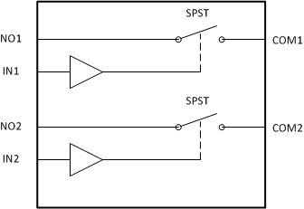
The TS3A4741 and TS3A4742 are bi-directional, 2-channel single-pole/single-throw (SPST) analog switches with low ON-state resistance (Ron), low-voltage, that operate from a single 1.6-V to 3.6-V supply. These devices have fast switching speeds, handle rail-to-rail analog signals, and consume very low quiescent power.
The digital logic input is 1.8-V CMOS compatible when using a single 3-V supply.
The TS3A4741 has two normally open (NO) switches, and the TS3A4742 has two normally closed (NC) switches.
8.2 Functional Block Diagram

8.3 Feature Description
The TS3A4741 and TS3A4742 has a low on resistance and high current handling capability up to 100 mA continuous current so it can be used for power sequencing and routing with minimal losses. The switch is also bi-directional with fast switching times in the 10 ns range which allows data acquisition and communication between multiple devices.
With a 3-V supply these devices are compatible with standard 1.8-V CMOS logic.
8.4 Device Functional Modes
Table 1. Function Table
| IN | NO to COM, COM to NO (TS3A4741) |
NC to COM, COM to NC (TS3A4742) |
|---|---|---|
| L | OFF | ON |
| H | ON | OFF |