SCDS228F AUGUST 2006 – December 2015 TS3A4741 , TS3A4742
UNLESS OTHERWISE NOTED, this document contains PRODUCTION DATA.
- 1 Features
- 2 Applications
- 3 Description
- 4 Revision History
- 5 Pin Configuration and Functions
- 6 Specifications
- 7 Parameter Measurement Information
- 8 Detailed Description
- 9 Application and Implementation
- 10Power Supply Recommendations
- 11Layout
- 12Device and Documentation Support
- 13Mechanical, Packaging, and Orderable Information
Package Options
Mechanical Data (Package|Pins)
Thermal pad, mechanical data (Package|Pins)
- DCN|8
Orderable Information
11 Layout
11.1 Layout Guidelines
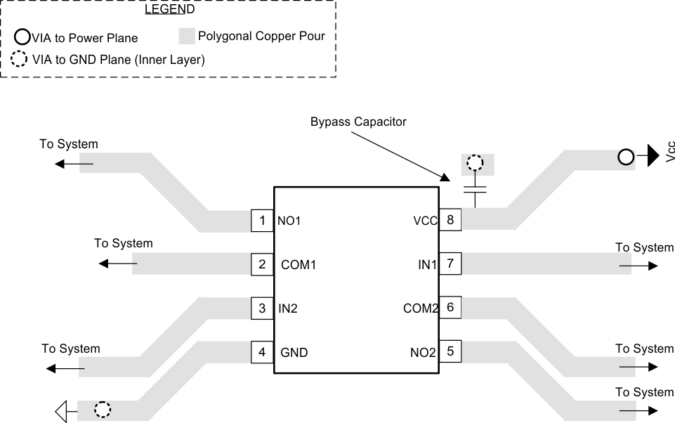
High-speed switches require proper layout and design procedures for optimum performance. Reduce stray inductance and capacitance by keeping traces short and wide. Ensure that bypass capacitors are as close to the device as possible. Use large ground planes where possible.
11.2 Layout Example
 Figure 21. PCB Layout Example