SLUSCU6C August 2017 – January 2020 UCC256301
PRODUCTION DATA.
- 1 Features
- 2 Applications
- 3 Description
- 4 Revision History
- 5 Pin Configuration and Functions
- 6 Specifications
-
7 Detailed Description
- 7.1 Overview
- 7.2 Functional Block Diagram
- 7.3
Feature Description
- 7.3.1 Hybrid Hysteretic Control
- 7.3.2 Regulated 12-V Supply
- 7.3.3 Feedback Chain
- 7.3.4 Optocoupler Feedback Signal Input and Bias
- 7.3.5 System External Shut Down
- 7.3.6 Pick Lower Block and Soft Start Multiplexer
- 7.3.7 Pick Higher Block and Burst Mode Multiplexer
- 7.3.8 VCR Comparators
- 7.3.9 Resonant Capacitor Voltage Sensing
- 7.3.10 Resonant Current Sensing
- 7.3.11 Bulk Voltage Sensing
- 7.3.12 Output Voltage Sensing
- 7.3.13 High Voltage Gate Driver
- 7.3.14 Protections
- 7.4 Device Functional Modes
-
8 Application and Implementation
- 8.1 Application Information
- 8.2
Typical Application
- 8.2.1 Design Requirements
- 8.2.2
Detailed Design Procedure
- 8.2.2.1 LLC Power Stage Requirements
- 8.2.2.2 LLC Gain Range
- 8.2.2.3 Select Ln and Qe
- 8.2.2.4 Determine Equivalent Load Resistance
- 8.2.2.5 Determine Component Parameters for LLC Resonant Circuit
- 8.2.2.6 LLC Primary-Side Currents
- 8.2.2.7 LLC Secondary-Side Currents
- 8.2.2.8 LLC Transformer
- 8.2.2.9 LLC Resonant Inductor
- 8.2.2.10 LLC Resonant Capacitor
- 8.2.2.11 LLC Primary-Side MOSFETs
- 8.2.2.12 Design Considerations for Adaptive Dead-Time
- 8.2.2.13 LLC Rectifier Diodes
- 8.2.2.14 LLC Output Capacitors
- 8.2.2.15 HV Pin Series Resistors
- 8.2.2.16 BLK Pin Voltage Divider
- 8.2.2.17 BW Pin Voltage Divider
- 8.2.2.18 ISNS Pin Differentiator
- 8.2.2.19 VCR Pin Capacitor Divider
- 8.2.2.20 Burst Mode Programming
- 8.2.2.21 Soft-Start Capacitor
- 8.2.3 Application Curves
- 9 Power Supply Recommendations
- 10Layout
- 11Device and Documentation Support
- 12Mechanical, Packaging, and Orderable Information
Package Options
Mechanical Data (Package|Pins)
- DDB|14
Thermal pad, mechanical data (Package|Pins)
Orderable Information
3 Description
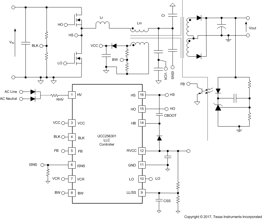
The UCC256301 is a fully featured LLC controller with integrated high-voltage gate driver. It has been designed to pair with a PFC stage to provide a complete power system using a minimum of external components. The resulting power system is designed to meet the most stringent requirements for standby power without the need for a separate standby power converter, and with PFC stage running all the time. UCC256301 includes a range of features designed to make LLC converter operation well controlled and robust. This device aims to unburden the LLC designer and allow mainstream applications to benefit from efficiency advantages of the LLC topology.
UCC256301 uses hybrid hysteretic control to provide best in class line and load transient response. The control effort is approximately linear proportional to average input current in one cycle. The control makes the open loop transfer function a first order system so that it’s very easy to compensate. The system is always stable with proper frequency compensation.
UCC256301 provides a high efficient burst mode with consistent burst power level during each burst on cycle. The burst power level is programmable and adaptively changes with input voltage, making the optimization of efficiency very easy.
Device Information(1)
| PART NUMBER | PACKAGE | BODY SIZE (NOM) |
|---|---|---|
| UCC256301 | SOIC (16) | 9.9 mm x 3.9 mm |
- For all available packages, see the orderable addendum at the end of the data sheet.
Simplified Schematic
