SLUSCU6C August 2017 – January 2020 UCC256301
PRODUCTION DATA.
- 1 Features
- 2 Applications
- 3 Description
- 4 Revision History
- 5 Pin Configuration and Functions
- 6 Specifications
-
7 Detailed Description
- 7.1 Overview
- 7.2 Functional Block Diagram
- 7.3
Feature Description
- 7.3.1 Hybrid Hysteretic Control
- 7.3.2 Regulated 12-V Supply
- 7.3.3 Feedback Chain
- 7.3.4 Optocoupler Feedback Signal Input and Bias
- 7.3.5 System External Shut Down
- 7.3.6 Pick Lower Block and Soft Start Multiplexer
- 7.3.7 Pick Higher Block and Burst Mode Multiplexer
- 7.3.8 VCR Comparators
- 7.3.9 Resonant Capacitor Voltage Sensing
- 7.3.10 Resonant Current Sensing
- 7.3.11 Bulk Voltage Sensing
- 7.3.12 Output Voltage Sensing
- 7.3.13 High Voltage Gate Driver
- 7.3.14 Protections
- 7.4 Device Functional Modes
-
8 Application and Implementation
- 8.1 Application Information
- 8.2
Typical Application
- 8.2.1 Design Requirements
- 8.2.2
Detailed Design Procedure
- 8.2.2.1 LLC Power Stage Requirements
- 8.2.2.2 LLC Gain Range
- 8.2.2.3 Select Ln and Qe
- 8.2.2.4 Determine Equivalent Load Resistance
- 8.2.2.5 Determine Component Parameters for LLC Resonant Circuit
- 8.2.2.6 LLC Primary-Side Currents
- 8.2.2.7 LLC Secondary-Side Currents
- 8.2.2.8 LLC Transformer
- 8.2.2.9 LLC Resonant Inductor
- 8.2.2.10 LLC Resonant Capacitor
- 8.2.2.11 LLC Primary-Side MOSFETs
- 8.2.2.12 Design Considerations for Adaptive Dead-Time
- 8.2.2.13 LLC Rectifier Diodes
- 8.2.2.14 LLC Output Capacitors
- 8.2.2.15 HV Pin Series Resistors
- 8.2.2.16 BLK Pin Voltage Divider
- 8.2.2.17 BW Pin Voltage Divider
- 8.2.2.18 ISNS Pin Differentiator
- 8.2.2.19 VCR Pin Capacitor Divider
- 8.2.2.20 Burst Mode Programming
- 8.2.2.21 Soft-Start Capacitor
- 8.2.3 Application Curves
- 9 Power Supply Recommendations
- 10Layout
- 11Device and Documentation Support
- 12Mechanical, Packaging, and Orderable Information
Package Options
Mechanical Data (Package|Pins)
- DDB|14
Thermal pad, mechanical data (Package|Pins)
Orderable Information
7.4.6 Waveform Generator State Machine
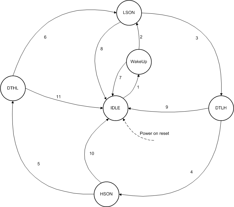
The waveform generator module consists of a state machine that implements hybrid hysteretic control, adaptive dead time, and ZCS protection. Each cycle of LLC operation is broken down into 4 separate periods: HSON, DTHL, LSON, and DTLH. In addition, there is an IDLE state and a WAKEUP state.
The initial state of this state machine is IDLE. In IDLE state, the system is operating in a low power mode. When WaveGenEn command is received, the state machine enters WAKEUP state to turn on various circuit blocks. Once the WAKEUP timer is expired, the system enters LSON (low side on) state. LSON state is followed by DTLH (dead time high to low) state, which is the dead time state. After DTLH state, the high side turns on and system enters HSON. HSON state is followed by DTHL (dead time low to high) state. After DTHL, the system goes back to LSON state again.
There are minimum and maximum timers in each of the states. The state transition conditions and descriptions are discussed in detail below.
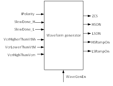
 Figure 52. Waveform Generator State Machine Block Diagram
 Table 4 summarizes the inputs and outputs of the Waveform Generator State Machine Block Diagram
NOTE
OVP and OCP1 faults are not listed here. But they are processed in the wave gen state machine before handled to system states and faults state machine.
Table 4. Waveform Generator State Machine Inputs and Outputs
| SIGNAL NAME | I/O | DESCRIPTION |
| IPolarity | I | Polarity of the resonant current (Note: this signal has a 1us blanking time during dead time. IPolarity signal listed here is after blanking. See ISNS section for details.) |
| SlewDone_H | I | Primary side switch node completes slewing from low to high |
| SlewDone_L | I | Primary side switch node completes slewing from high to low |
| VcrHigherThanVthh | I | VCR voltage is higher than the high threshold Vthh |
| VcrLowerThanVthl | I | VCR voltage is lower than the low threshold Vthl |
| VcrHighThanVcm | I | VCR voltage is high than the common mode voltage Vcm |
| WaveGenEn | I | Waveform generator enable |
| ZCS | O | Zero current switching is detected |
| HSON | O | High side gate driver on |
| LSON | O | Low side gate driver on |
| HSRampOn | O | High side compensation current ramp on |
| LSRampOn | O | Low side compensation current ramp on |
The state machine is shown in Figure 53 and the description of the states and state transition conditions are in Table 5.
 Figure 53. Waveform Generator State Machine
 Table 5. States in Waveform Generator State Machine
| STATE | OUTPUT STATUS | DESCRIPTION |
|---|---|---|
| IDLE | HSON = 0
LSON = 0 HSRampOn = 0 LSRampOn = 0 ZCS = 0 |
Both high side and low side are off in this state. Various circuits are operating in low power mode. This is the first state after POR. During burst off period, the system is in IDLE state as well. Upon entering IDLE state, load burst cycle counter, switching cycle counter, OCP1 counter, and OVP counter. Load startup cycle counter if WaveGenEn_Rising = 1 |
| WakeUp | HSON = 0
LSON = 0 HSRampOn = 0 LSRampOn = 0 ZCS = 0 |
In this state, internal circuits wake up from low power mode. |
| LSON | HSON = 0
LSON = 1 HSRampOn = 0 LSRampOn = 1 ZCS = 0 or 1 |
In this state, the low side gate turns on; the low side ramp current source turns on. ZCS may be 0 or 1 depends on the detected result. More details will be described in ZCS section. Enable low side on timer. |
| DTLH | HSON = 0
LSON = 0 HSRampOn = 1 LSRampOn = 0 ZCS = 0 or 1 |
Dead time from low side on to high side on. Low side ramp current source turns off. High side ramp current source turns on. Enable dead time timer. |
| HSON | HSON = 1
LSON = 0 HSRampOn = 1 LSRampOn = 0 ZCS = 0 or 1 |
In this state, the high side gate turns on; the high side ramp current source turns on. ZCS may be 0 or 1 depends on the detected result. More details will be described in ZCS section. Enable high side on timer. |
| DTHL | HSON = 0
LSON = 0 HSRampOn = 0 LSRampOn = 1 ZCS = 0 or 1 |
Dead time from high side on to low side on. High side ramp current source turns off. Low side ramp current source turns on. Enable dead time timer. |
Table 6. Waveform Generator State Machine State Transition Conditions
| STATE TRANSITION CONDITION | DESCRIPTION |
| 1 | WaveGenEn = 1 and FBLessThanBMT = 0 and minimum IDLE time expired |
| 2 | Wake up time expired |
| 3 | (VcrLowerThanVthl = 1 or LSON max timer expired) and LSON min timer expired |
| 4 | StartUpCounterExpired = 0 and DTStartUpTimerExpired = 1
DTMaxTimerExpired = 1 SlewDone_H = 1 SlewDone_H = 1 and MeasuredDTExpired = 1; (Note: this condition and the condition above is selectable using a trim bit, depending on whether dead time measure and match feature is wanted) IPolarityFallingEdgeDetected = 1 |
| 5 | (VcrHigherThanVthh = 1 or HSON max timer expired) and HSON min timer expired |
| 6 | StartUpCounterExpired = 0 and DTStartUpTimerExpired = 1
DTMaxTimerExpired = 1 SlewDone_L = 1 IPolarityFallingEdgeDetected = 1 |
| 7 | WaveGenEn = 0 |
| 8 | WaveGenEn = 0
(VcrLowerThanVthl = 1 or LSON max timer expired) and LSON min timer expired and (OCP1 counter expire or OVP counter expire) |
| 9 | WaveGenEn = 0 |
| 10 | WaveGenEn = 0
BurstModeCountExpire = 1 and VcrHigherThanVcm = 1 and FBLessThanBMT = 1 and HSON min time expired |
| 11 | WaveGenEn = 0 |
Table 7. Waveform Generator State Machine Internal Counters and Timers
| INTERNAL VARIABLE | DESCRIPTION |
| Switching cycle counter | This counter counts the switching cycle |
| OVP counter | Bias Winding Overvoltage counter. The counter decrements every time a Bias Winding Overvoltage occurs |
| Startup counter | Startup Counter. Counter gets set to 15 when wave generator enable toggles from low to high, and then decrements every switching cycle. When the count hits 0, the dead time state is no longer permitted to be exited via the startup dead time expiration. |
| Burst cycle counter | Burst counter. Counter gets set to 15 and then decrements every switching cycle until it hits ‘0’. If FBLessThanBMT = 1 when the counter is ‘0’, the switcher will stop until FBLessThanBMT = 0. |
| OCP1 counter | OCP1 counter. Counter gets set to 4 and then decrements every switching cycle when OCP1 occurs, until it hits ‘0’ |
| Wakeup timer | Wakeup state timer |
| DT max timer | Maximum dead time timer |
| Startup dead time max timer | Dead time max clamp for the first few start up cycles before the startup counter expires |
| Gate on min timer | Minimum gate on time timer |
| Gate on max timer | Maximum gate on time timer |