SGLS245F May 2004 – April 2025 UCC2813-0-Q1 , UCC2813-1-Q1 , UCC2813-2-Q1 , UCC2813-3-Q1 , UCC2813-4-Q1 , UCC2813-5-Q1
PRODUCTION DATA
- 1
- 1 Features
- 2 Applications
- 3 Description
- 4 Device Comparison Table
- 5 Pin Configuration and Functions
- 6 Specifications
-
7 Detailed Description
- 7.1 Overview
- 7.2 Functional Block Diagram
- 7.3
Feature Description
- 7.3.1 Detailed Pin Descriptions
- 7.3.2 Undervoltage Lockout (UVLO)
- 7.3.3 Self-Biasing, Active Low Output
- 7.3.4 Reference Voltage
- 7.3.5 Oscillator
- 7.3.6 Synchronization
- 7.3.7 PWM Generator
- 7.3.8 Minimum Off-Time Adjustment (Dead-Time Control)
- 7.3.9 Leading Edge Blanking
- 7.3.10 Minimum Pulse Width
- 7.3.11 Current Limiting
- 7.3.12 Overcurrent Protection and Full-Cycle Restart
- 7.3.13 Soft Start
- 7.3.14 Slope Compensation
- 7.4 Device Functional Modes
-
8 Application and Implementation
- 8.1 Application Information
- 8.2
Typical Application
- 8.2.1 Design Requirements
- 8.2.2
Detailed Design Procedure
- 8.2.2.1 Bulk Capacitor Calculation
- 8.2.2.2 Transformer Design
- 8.2.2.3 MOSFET and Output Diode Selection
- 8.2.2.4 Output Capacitor Calculation
- 8.2.2.5 Current Sensing Network
- 8.2.2.6 Gate Drive Resistor
- 8.2.2.7 REF Bypass Capacitor
- 8.2.2.8 RT and CT
- 8.2.2.9 Start-Up Circuit
- 8.2.2.10 Voltage Feedback Compensation Procedure
- 8.2.3 Application Curves
- 8.3 Power Supply Recommendations
- 8.4 Layout
- 9 Device and Documentation Support
- 10Revision History
- 11Mechanical, Packaging, and Orderable Information
Package Options
Refer to the PDF data sheet for device specific package drawings
Mechanical Data (Package|Pins)
- D|8
Thermal pad, mechanical data (Package|Pins)
Orderable Information
7.3.4 Reference Voltage
The traditional 5-V band-gap-derived reference voltage of the UC3842 family can be also found on the UCC2813-[0,1,2,4]-Q1 devices. However, the reference voltage of the UCC2813-[3,5]-Q1 devices is 4 V. This change was necessary to facilitate operation with input supply voltages below 5 V. Many of the reference voltage specifications are similar to the UC3842 devices although the test conditions have been changed, indicative of lower-current PWM applications. Similar to their bipolar counterparts, the BiCMOS devices internally pull the reference voltage low during UVLO, which can be used as a logic status indication.
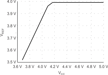
The 4-V reference voltage on the UCC2813-[3,5]-Q1 is derived from the supply voltage (VVCC) and requires about 0.5 V of headroom to maintain regulation. Whenever VVCC is below approximately 4.5 V, the reference voltage also drops outside of its specified range for normal operation. The relationship between VVCC and VREF during this excursion is shown in Figure 7-4.
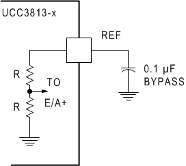
The noninverting input to the error amplifier is tied to one-half of the controller's reference voltage (VREF). This input is 2 V on the UCC2813-[3,5]-Q1 and 2.5 V on the higher reference voltage parts: the UCC2813-[0,1,2,4]-Q1.
 Figure 7-4 UCC2813-3-Q1 REF Output vs VVCC
 Figure 7-5 Required Reference Bypass Minimum Capacitance