SGLS245F May 2004 – April 2025 UCC2813-0-Q1 , UCC2813-1-Q1 , UCC2813-2-Q1 , UCC2813-3-Q1 , UCC2813-4-Q1 , UCC2813-5-Q1
PRODUCTION DATA
- 1
- 1 Features
- 2 Applications
- 3 Description
- 4 Device Comparison Table
- 5 Pin Configuration and Functions
- 6 Specifications
-
7 Detailed Description
- 7.1 Overview
- 7.2 Functional Block Diagram
- 7.3
Feature Description
- 7.3.1 Detailed Pin Descriptions
- 7.3.2 Undervoltage Lockout (UVLO)
- 7.3.3 Self-Biasing, Active Low Output
- 7.3.4 Reference Voltage
- 7.3.5 Oscillator
- 7.3.6 Synchronization
- 7.3.7 PWM Generator
- 7.3.8 Minimum Off-Time Adjustment (Dead-Time Control)
- 7.3.9 Leading Edge Blanking
- 7.3.10 Minimum Pulse Width
- 7.3.11 Current Limiting
- 7.3.12 Overcurrent Protection and Full-Cycle Restart
- 7.3.13 Soft Start
- 7.3.14 Slope Compensation
- 7.4 Device Functional Modes
-
8 Application and Implementation
- 8.1 Application Information
- 8.2
Typical Application
- 8.2.1 Design Requirements
- 8.2.2
Detailed Design Procedure
- 8.2.2.1 Bulk Capacitor Calculation
- 8.2.2.2 Transformer Design
- 8.2.2.3 MOSFET and Output Diode Selection
- 8.2.2.4 Output Capacitor Calculation
- 8.2.2.5 Current Sensing Network
- 8.2.2.6 Gate Drive Resistor
- 8.2.2.7 REF Bypass Capacitor
- 8.2.2.8 RT and CT
- 8.2.2.9 Start-Up Circuit
- 8.2.2.10 Voltage Feedback Compensation Procedure
- 8.2.3 Application Curves
- 8.3 Power Supply Recommendations
- 8.4 Layout
- 9 Device and Documentation Support
- 10Revision History
- 11Mechanical, Packaging, and Orderable Information
Package Options
Refer to the PDF data sheet for device specific package drawings
Mechanical Data (Package|Pins)
- D|8
Thermal pad, mechanical data (Package|Pins)
Orderable Information
6.5 Electrical Characteristics
Unless otherwise stated, these specifications apply for –40°C ≤ TA ≤ 125°C , TJ = TA; VVCC = 10 V(1); RT = 100 kΩ from REF to RC; CT = 330 pF from RC to GND; 0.1-µF capacitor from VCC to GND; 0.1-µF capacitor from VREF to GND.
| PARAMETER | TEST CONDITIONS | MIN | TYP | MAX | UNIT | |
|---|---|---|---|---|---|---|
| REFERENCE | ||||||
| Output voltage | TJ = 25°C, I = 0.2 mA, UCC2813-[0,1,2,4]-Q1 | 4.925 | 5 | 5.075 | V | |
| TJ = 25°C, I = 0.2 mA, UCC2813-[3,5]-Q1 | 3.94 | 4 | 4.06 | |||
| Load regulation | 0.2 mA < I < 5 mA | 10 | 30 | mV | ||
| Total variation | UCC2813-[0,1,2,4]-Q1(5) | 4.84 | 5 | 5.1 | V | |
| UCC2813-[3,5]-Q1(5) | 3.84 | 4 | 4.08 | |||
| Output noise voltage | 10 Hz ≤ f ≤ 10 kHz, TJ = 25°C(7) | 70 | µV | |||
| Long term stability | TA = 125°C, 1000 hours(7) | 5 | mV | |||
| Output short circuit current | –5 | –35 | mA | |||
| OSCILLATOR | ||||||
| Oscillator frequency | UCC2813-[0,1,2,4]-Q1(2) | 40 | 46 | 52 | kHz | |
| UCC2813-[3,5]-Q1(2) | 26 | 31 | 36 | |||
| Temperature stability | See note (7) | 2.5% | ||||
| Amplitude peak-to-peak | 2.25 | 2.4 | 2.55 | V | ||
| Oscillator peak voltage | 2.45 | V | ||||
| ERROR AMPLIFIER | ||||||
| Input voltage | VCOMP = 2.5 V; UCC2813-[0,1,2,4]-Q1 | 2.42 | 2.5 | 2.56 | V | |
| VCOMP = 2 V; UCC2813-[3,5]-Q1 | 1.92 | 2 | 2.05 | |||
| Input bias current | –2 | 2 | µA | |||
| Open loop voltage gain | 60 | 80 | dB | |||
| COMP sink current | VFB = 2.7 V, VCOMP = 1.1 V | 0.3 | 3.5 | mA | ||
| COMP source current | VFB = 1.8 V, VCOMP = VREF – 1.2 V | –0.2 | –0.5 | –0.8 | mA | |
| Gain-bandwidth product | See note (7) | 2 | MHz | |||
| PWM | ||||||
| Maximum duty cycle | UCC2813-[0,2,3]-Q1 | 97 | 99 | 100 | % | |
| UCC2813-[1,4,5]-Q1 | 48 | 49 | 50 | |||
| Minimum duty cycle | VCOMP = 0 V | 0 | % | |||
| CURRENT SENSE | ||||||
| Gain | See note (3) | 1.1 | 1.65 | 1.8 | V/V | |
| Maximum input signal | VCOMP = 5 V(4) | 0.9 | 1 | 1.1 | V | |
| Input bias current | –200 | 200 | nA | |||
| CS blank time | 50 | 100 | 150 | ns | ||
| Over-current threshold | 1.32 | 1.55 | 1.7 | V | ||
| COMP to CS offset | VCS = 0 V | 0.45 | 0.9 | 1.35 | V | |
| OUTPUT | ||||||
| OUT low level | I = 20 mA, all parts | 0.1 | 0.4 | V | ||
| I = 200 mA, all parts | 0.35 | 0.9 | ||||
| I = 50 mA, VVCC = 5 V, UCC2813-[3,5]-Q1 | 0.15 | 0.4 | ||||
| I = 20 mA, VCC = 0 V, all parts | 0.7 | 1.2 | ||||
| VVCC – OUT | OUT high Vsat | I = –20 mA, all parts | 0.15 | 0.4 | V | |
| I = –200 mA, all parts | 1 | 1.9 | ||||
| I = –50 mA, VVCC = 5 V, UCC2813-[3,5]-Q1 | 0.4 | 0.9 | ||||
| Rise time | CL = 1 nF | 41 | 70 | ns | ||
| Fall time | CL = 1 nF | 44 | 75 | ns | ||
| UNDERVOLTAGE LOCKOUT | ||||||
| Start threshold (6) | UCC2813-0-Q1 | 6.6 | 7.2 | 7.8 | V | |
| UCC2813-1-Q1 | 8.6 | 9.4 | 10.2 | |||
| UCC2813-[2,4]-Q1 | 11.5 | 12.5 | 13.5 | |||
| UCC2813-[3,5]-Q1 | 3.7 | 4.1 | 4.5 | |||
| Stop threshold (6) | UCC2813-0-Q1 | 6.3 | 6.9 | 7.5 | V | |
| UCC2813-1-Q1 | 6.8 | 7.4 | 8 | |||
| UCC2813-[2,4]-Q1 | 7.6 | 8.3 | 9 | |||
| UCC2813-[3,5]-Q1 | 3.2 | 3.6 | 4 | |||
| Start to stop hysteresis | UCC2813-0-Q1 | 0.12 | 0.3 | 0.48 | V | |
| UCC2813-1-Q1 | 1.6 | 2 | 2.4 | |||
| UCC2813-[2,4]-Q1 | 3.5 | 4.2 | 5.1 | |||
| UCC2813-[3,5]-Q1 | 0.2 | 0.5 | 0.8 | |||
| SOFT START | ||||||
| COMP rise time | VFB = 1.8 V, Rise from 0.5 V to REF – 1 V | 4 | 10 | ms | ||
| OVERALL | ||||||
| Start-up current | VVCC < start threshold | 0.1 | 0.23 | mA | ||
| Operating supply current | VFB = 0 V, VCS = 0 V, VRC = 0 V | 0.5 | 1.2 | mA | ||
| VCC internal Zener voltage(6) | IVCC = 10 mA(8) | 12 | 13.5 | 15 | V | |
| VCC internal Zener voltage minus start-threshold voltage (6) | UCC2813-[2,4]-Q1(8) | 0.5 | 1 | V | ||
(1) Adjust VCC above the start threshold before setting at 10 V.
(2) Output frequency for the UCC2813-[0,2,3]-Q1 device is the oscillator frequency. Output frequency for the UCC2813-[1,4,5]-Q1 device is one-half the oscillator frequency.
(3) Gain is defined by:
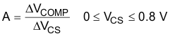 .
.
.(4) Parameter measured at trip point of latch with FB at 0 V.
(5) Total variation includes temperature stability and load regulation.
(6) Start threshold, stop threshold, and Zener-shunt thresholds track one another.
(7) Ensured by design. Not 100% tested in production.
(8) The device is fully operating in clamp mode as the forcing current is higher
than the normal operating supply current.