SLUSDT2C August 2019 – December 2020 UCC28740-Q1
PRODUCTION DATA
- 1 Features
- 2 Applications
- 3 Description
- 4 Revision History
- 5 Pin Configuration and Functions
- 6 Specifications
- 7 Detailed Description
-
8 Application and Implementation
- 8.1 Application Information
- 8.2 High Voltage Applications
- 8.3
Typical Application
- 8.3.1 Design Requirements
- 8.3.2
Detailed Design Procedure
- 8.3.2.1 Custom Design With WEBENCH® Tools
- 8.3.2.2 Standby Power Estimate and No-Load Switching Frequency
- 8.3.2.3 Input Bulk Capacitance and Minimum Bulk Voltage
- 8.3.2.4 35
- 8.3.2.5 Transformer Turns-Ratio, Inductance, Primary Peak Current
- 8.3.2.6 Transformer Parameter Verification
- 8.3.2.7 VS Resistor Divider, Line Compensation
- 8.3.2.8 Output Capacitance
- 8.3.2.9 VDD Capacitance, CVDD
- 8.3.2.10 Feedback Network Biasing
- 8.3.3 Application Curves
- 9 Power Supply Recommendations
- 10Layout
-
11Device and Documentation Support
- 11.1
Device Support
- 11.1.1 Development Support
- 11.1.2
Device Nomenclature
- 11.1.2.1 Capacitance Terms in Farads
- 11.1.2.2 Duty Cycle Terms
- 11.1.2.3 Frequency Terms in Hertz
- 11.1.2.4 Current Terms in Amperes
- 11.1.2.5 Current and Voltage Scaling Terms
- 11.1.2.6 Transformer Terms
- 11.1.2.7 Power Terms in Watts
- 11.1.2.8 Resistance Terms in Ohms
- 11.1.2.9 Timing Terms in Seconds
- 11.1.2.10 Voltage Terms in Volts
- 11.1.2.11 AC Voltage Terms in VRMS
- 11.1.2.12 Efficiency Terms
- 11.2 Documentation Support
- 11.3 Receiving Notification of Documentation Updates
- 11.4 Community Resources
- 11.5 Trademarks
- 11.1
Device Support
Package Options
Mechanical Data (Package|Pins)
- D|7
Thermal pad, mechanical data (Package|Pins)
Orderable Information
8.3.2.6 Transformer Parameter Verification
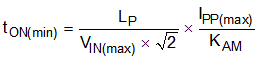
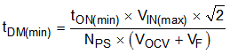
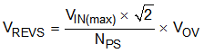
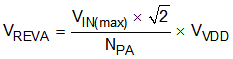
Because the selected transformer turns-ratio affects the MOSFET VDS and the secondary and auxiliary rectifier reverse voltages, a review of these voltages is important. In addition, internal timing constraints of the UCC28740-Q1 require a minimum on time of the MOSFET (tON) and a minimum demagnetization time (tDM) of the transformer in the high-line minimum-load condition. The selection of fMAX, LP, and RCS affects the minimum tON and tDM.
Equation 19 and Equation 20 determine the reverse voltage stresses on the secondary and auxiliary rectifiers. Stray inductance can impress additional voltage spikes upon these stresses and snubbers may be necessary.
For the MOSFET VDS peak voltage stress, an estimated leakage inductance voltage spike (VLK) is included.

Equation 22 determines if tON(min) exceeds the minimum tON target of 280 ns (maximum tCSLEB). Equation 23 verifies that tDM(min) exceeds the minimum tDM target of 1.2 µs.