SLUSDT2C August 2019 – December 2020 UCC28740-Q1
PRODUCTION DATA
- 1 Features
- 2 Applications
- 3 Description
- 4 Revision History
- 5 Pin Configuration and Functions
- 6 Specifications
- 7 Detailed Description
-
8 Application and Implementation
- 8.1 Application Information
- 8.2 High Voltage Applications
- 8.3
Typical Application
- 8.3.1 Design Requirements
- 8.3.2
Detailed Design Procedure
- 8.3.2.1 Custom Design With WEBENCH® Tools
- 8.3.2.2 Standby Power Estimate and No-Load Switching Frequency
- 8.3.2.3 Input Bulk Capacitance and Minimum Bulk Voltage
- 8.3.2.4 35
- 8.3.2.5 Transformer Turns-Ratio, Inductance, Primary Peak Current
- 8.3.2.6 Transformer Parameter Verification
- 8.3.2.7 VS Resistor Divider, Line Compensation
- 8.3.2.8 Output Capacitance
- 8.3.2.9 VDD Capacitance, CVDD
- 8.3.2.10 Feedback Network Biasing
- 8.3.3 Application Curves
- 9 Power Supply Recommendations
- 10Layout
-
11Device and Documentation Support
- 11.1
Device Support
- 11.1.1 Development Support
- 11.1.2
Device Nomenclature
- 11.1.2.1 Capacitance Terms in Farads
- 11.1.2.2 Duty Cycle Terms
- 11.1.2.3 Frequency Terms in Hertz
- 11.1.2.4 Current Terms in Amperes
- 11.1.2.5 Current and Voltage Scaling Terms
- 11.1.2.6 Transformer Terms
- 11.1.2.7 Power Terms in Watts
- 11.1.2.8 Resistance Terms in Ohms
- 11.1.2.9 Timing Terms in Seconds
- 11.1.2.10 Voltage Terms in Volts
- 11.1.2.11 AC Voltage Terms in VRMS
- 11.1.2.12 Efficiency Terms
- 11.2 Documentation Support
- 11.3 Receiving Notification of Documentation Updates
- 11.4 Community Resources
- 11.5 Trademarks
- 11.1
Device Support
Package Options
Mechanical Data (Package|Pins)
- D|7
Thermal pad, mechanical data (Package|Pins)
Orderable Information
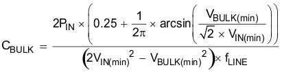
8.3.2.3 Input Bulk Capacitance and Minimum Bulk Voltage
Determine the minimum voltage on the input bulk capacitance, CB1 and CB2 total, in order to determine the maximum Np-to-Ns turns-ratio of the transformer. The input power of the converter based on target full-load efficiency, the minimum input RMS voltage, and the minimum AC input frequency determine the input capacitance requirement.
Maximum input power is determined based on IOCC, VOCV, VCBC (if used), and the full-load conversion-efficiency target.
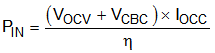
Equation 11 provides an accurate solution for the total input capacitance based on a target minimum bulk-capacitor voltage. Alternatively, to target a given input capacitance value, iterate the minimum capacitor voltage to achieve the target capacitance value.