SLUSAP2J March 2012 – November 2021 UCD3138
PRODUCTION DATA
- 1 Features
- 2 Applications
- 3 Description
- 4 Functional Block Diagram
- 5 Revision History
- 6 Device Comparison Table
- 7 Pin Configuration and Functions
- 8 Specifications
-
9 Detailed Description
- 9.1 Overview
- 9.2 ARM Processor
- 9.3 Memory
- 9.4 System Module
- 9.5
Feature Description
- 9.5.1 Sync FET Ramp and IDE Calculation
- 9.5.2 Automatic Mode Switching
- 9.5.3 DPWMC, Edge Generation, IntraMux
- 9.5.4 Filter
- 9.5.5 Communication Ports
- 9.5.6 Miscellaneous Analog
- 9.5.7 Package ID Information
- 9.5.8 Brownout
- 9.5.9 Global I/O
- 9.5.10 Temperature Sensor Control
- 9.5.11 I/O Mux Control
- 9.5.12 Current Sharing Control
- 9.5.13 Temperature Reference
- 9.6 Device Functional Modes
-
10Application and Implementation
- 10.1 Application Information
- 10.2
Typical Application
- 10.2.1 Design Requirements
- 10.2.2 Detailed Design Procedure
- 10.2.3 Application Curves
- 11Power Supply Recommendations
- 12Layout
- 13Device and Documentation Support
- 14Mechanical Packaging and Orderable Information
Package Options
Mechanical Data (Package|Pins)
Thermal pad, mechanical data (Package|Pins)
Orderable Information
8.6 Timing and Switching Characteristics
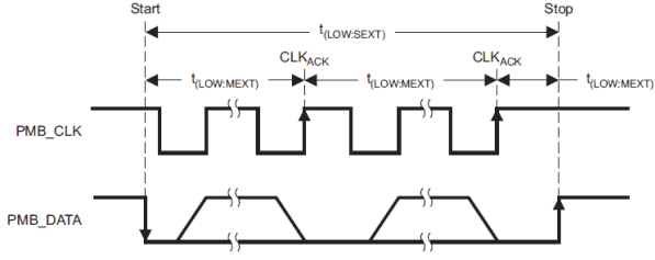
The timing characteristics and timing diagram for the communications interface that supports I2C, SMBus, and PMBus in Slave or Master mode are shown in PMBus/SMBus/I2C Timing, I2C/SMBus/PMBus Timing Diagram, and Bus Timing in Extended Mode. The numbers in PMBus/SMBus/I2C Timing arµe for 400 kHz operating frequency. However, the device supports all three speeds, standard (100 kHz), fast (400 kHz), and fast mode plus (1 MHz).
Table 8-1 PMBus/SMBus/I2C Timing
| PARAMETER | TEST CONDITIONS | MIN | TYP | MAX | UNIT | |
|---|---|---|---|---|---|---|
| Typical values at TA = 25°C and VCC = 3.3 V (unless otherwise noted) | ||||||
| fSMB | SMBus/PMBus operating frequency | Slave mode, SMBC 50% duty cycle | 100 | 1000 | kHz | |
| fI2C | I2C operating frequency | Slave mode, SCL 50% duty cycle | 100 | 1000 | kHz | |
| t(BUF) | Bus free time between start and stop | 1.3 | µs | |||
| t(HD:STA) | Hold time after (repeated) start(1) | 0.6 | µs | |||
| t(SU:STA) | Repeated start setup time(1) | 0.6 | µs | |||
| t(SU:STO) | Stop setup time(1) | 0.6 | µs | |||
| t(HD:DAT) | Data hold time | Receive mode | 0 | ns | ||
| t(SU:DAT) | Data setup time | 100 | ns | |||
| t(TIMEOUT) | Error signal/detect(2) | 35 | ms | |||
| t(LOW) | Clock low period | 1.3 | µs | |||
| t(HIGH) | Clock high period(3) | 0.6 | µs | |||
| t(LOW:SEXT) | Cumulative clock low slave extend time(4) | 25 | ms | |||
| tf | Clock/data fall time | Fall time tf = 0.9 VDD to (VILmax – 0.15) | 20 + 0.1 Cb(5) | 300 | ns | |
| tr | Clock/data rise time | Rise time tr = (VILmax – 0.15) to (VIHmin + 0.15) | 20 + 0.1 Cb(5) | 300 | ns | |
| Cb | Total capacitance of one bus line | 400 | pF | |||
(1) Fast mode, 400 kHz
(2) The device times out when any clock low exceeds t(TIMEOUT).
(3) t(HIGH), Max, is the minimum bus idle time. SMBC = SMBD = 1 for t > 50 ms causes reset of any transaction that is in progress. This specification is valid when the NC_SMB control bit remains in the default cleared state (CLK[0] = 0).
(4) t(LOW:SEXT) is the cumulative time a slave device is allowed to extend the clock cycles in one message from initial start to the stop.
(5) Cb (pF)
 Figure 8-1 I2C/SMBus/PMBus Timing Diagram
 Figure 8-2 Bus Timing in Extended Mode