SLUSAP2J March 2012 – November 2021 UCD3138
PRODUCTION DATA
- 1 Features
- 2 Applications
- 3 Description
- 4 Functional Block Diagram
- 5 Revision History
- 6 Device Comparison Table
- 7 Pin Configuration and Functions
- 8 Specifications
-
9 Detailed Description
- 9.1 Overview
- 9.2 ARM Processor
- 9.3 Memory
- 9.4 System Module
- 9.5
Feature Description
- 9.5.1 Sync FET Ramp and IDE Calculation
- 9.5.2 Automatic Mode Switching
- 9.5.3 DPWMC, Edge Generation, IntraMux
- 9.5.4 Filter
- 9.5.5 Communication Ports
- 9.5.6 Miscellaneous Analog
- 9.5.7 Package ID Information
- 9.5.8 Brownout
- 9.5.9 Global I/O
- 9.5.10 Temperature Sensor Control
- 9.5.11 I/O Mux Control
- 9.5.12 Current Sharing Control
- 9.5.13 Temperature Reference
- 9.6 Device Functional Modes
-
10Application and Implementation
- 10.1 Application Information
- 10.2
Typical Application
- 10.2.1 Design Requirements
- 10.2.2 Detailed Design Procedure
- 10.2.3 Application Curves
- 11Power Supply Recommendations
- 12Layout
- 13Device and Documentation Support
- 14Mechanical Packaging and Orderable Information
Package Options
Mechanical Data (Package|Pins)
Thermal pad, mechanical data (Package|Pins)
Orderable Information
9.5.4.2 Fault Multiplexer
In order to allow a flexible way of mapping several fault triggering sources to all the DPWMs channels, the UCD3138 provides an extensive array of multiplexers that are united under the name Fault Mux module.
The Fault Mux Module supports the following types of mapping between all the sources of fault and all different fault response mechanism inside each DPWM module.
- Many fault sources mapped to a single fault response mechanism. For instance an analog comparator in charge of over voltage protection, a digital comparator in charge of over current protection and an external digital fault pin can be all mapped to a fault-A signal connected to a single FAULT MODULE and shut down DPWM1-A.
- A single fault source can be mapped to many fault response mechanisms inside many DPWM modules. For instance an analog comparator in charge of over current protection can be mapped to DPWM-0 through DPWM-3 by way of several fault modules.
- Many fault sources can be mapped to many fault modules inside many DPWM modules.
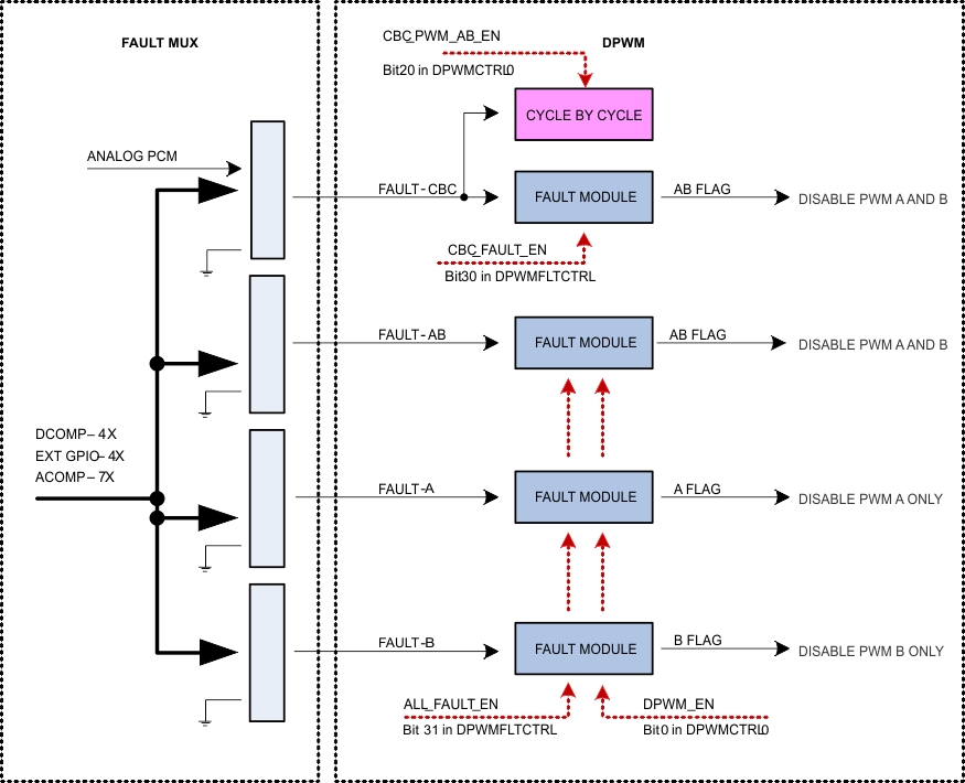
The Fault Mux Module provides a multitude of fault protection functions within the UCD3138 high-speed loop (front end control, filter, DPWM and loop Mux modules). The Fault Mux Module allows highly configurable fault generation based on digital comparators, high-speed analog comparators and external fault pins. Each of the fault inputs to the DPWM modules can be configured to one or any combination of the fault events provided in the Fault Mux Module.
Each one of the DPWM engines has four fault modules. The modules are called CBC fault module, AB fault module, A fault module and B fault module.
The internal circuitry in all the four fault modules is identical, and the difference between the modules is limited to the way the modules are attached to the DPWMs.
 Figure 9-10 Fault Module
All fault modules provide immediate fault detection but only once per DPWM switching cycle. Each one of the fault modules own a separate max_count and the fault flag will be set only if sequential cycle-by-cycle faults count exceeds max_count.
Once the fault flag is set DPWMs need to be disabled by DPWM_EN going low in order to clear the fault flags.
All four Fault Modules share the same DPWM_EN control, all fault flags (output of Fault Modules) will be cleared simultaneously.
All four Fault Modules share the same global FAULT_EN as well. Therefore a specific Fault Module cannot be enabled/ disabled separately.
 Figure 9-11 Cycle by Cycle Block
Unlike fault modules, only one cycle by cycle block is available in each DPWM module.
The cycle by cycle block works in conjunction with CBC Fault Module and enables DPWM reaction to signals arriving from analog peak current mode (PCM) module.
The fault Mux module supports the following basic functions:
- 4 digital comparators using the EADC as a source with programmable thresholds and fault generation
- Configuration for 7 high-speed analog comparators with programmable thresholds and fault generation
- External GPIO detection control with programmable fault generation
- Configurable DPWM fault generation for DPWM current limit fault, DPWM overvoltage detection fault, DPWM A external fault, DPWM B external fault and DPWM IDE flag
- Clock failure detection for high and low frequency oscillator blocks
- Discontinuous conduction mode detection
 Figure 9-12 Fault Mux Block Diagram