SLUSAP2J March 2012 – November 2021 UCD3138
PRODUCTION DATA
- 1 Features
- 2 Applications
- 3 Description
- 4 Functional Block Diagram
- 5 Revision History
- 6 Device Comparison Table
- 7 Pin Configuration and Functions
- 8 Specifications
-
9 Detailed Description
- 9.1 Overview
- 9.2 ARM Processor
- 9.3 Memory
- 9.4 System Module
- 9.5
Feature Description
- 9.5.1 Sync FET Ramp and IDE Calculation
- 9.5.2 Automatic Mode Switching
- 9.5.3 DPWMC, Edge Generation, IntraMux
- 9.5.4 Filter
- 9.5.5 Communication Ports
- 9.5.6 Miscellaneous Analog
- 9.5.7 Package ID Information
- 9.5.8 Brownout
- 9.5.9 Global I/O
- 9.5.10 Temperature Sensor Control
- 9.5.11 I/O Mux Control
- 9.5.12 Current Sharing Control
- 9.5.13 Temperature Reference
- 9.6 Device Functional Modes
-
10Application and Implementation
- 10.1 Application Information
- 10.2
Typical Application
- 10.2.1 Design Requirements
- 10.2.2 Detailed Design Procedure
- 10.2.3 Application Curves
- 11Power Supply Recommendations
- 12Layout
- 13Device and Documentation Support
- 14Mechanical Packaging and Orderable Information
Package Options
Mechanical Data (Package|Pins)
Thermal pad, mechanical data (Package|Pins)
Orderable Information
12.2.2 UCD3138 and UCD3138064 64 Pin
 Figure 12-12 Power and Ground
Schematic for UCD3138 and UCD3138064 64 Pin
Figure 12-12 Power and Ground
Schematic for UCD3138 and UCD3138064 64 PinTable 12-2 Power and Ground Connection Components for UCD3138 and UCD3138064 64 Pin
| COMPONENT | VALUE |
|---|---|
| C1 | 4.7 µF |
| C2 | 10 nF |
| C3 | 2.2 µF |
| R1 | 2.2 kΩ |
| C4 | 4.7 µF |
| C5 | 10 nF |
| C6 | 4.7 µF |
| C7 | 10 nF |
| C8 | 1 µF |
| C9 | 10 nF |
| C10 | 4.7 µF |
| R2 | 1 Ω |
| C11 | 10 µF |
| C12 | 10 µF |
| C13 | 2.2 µF |
| C14 | 10 nF |
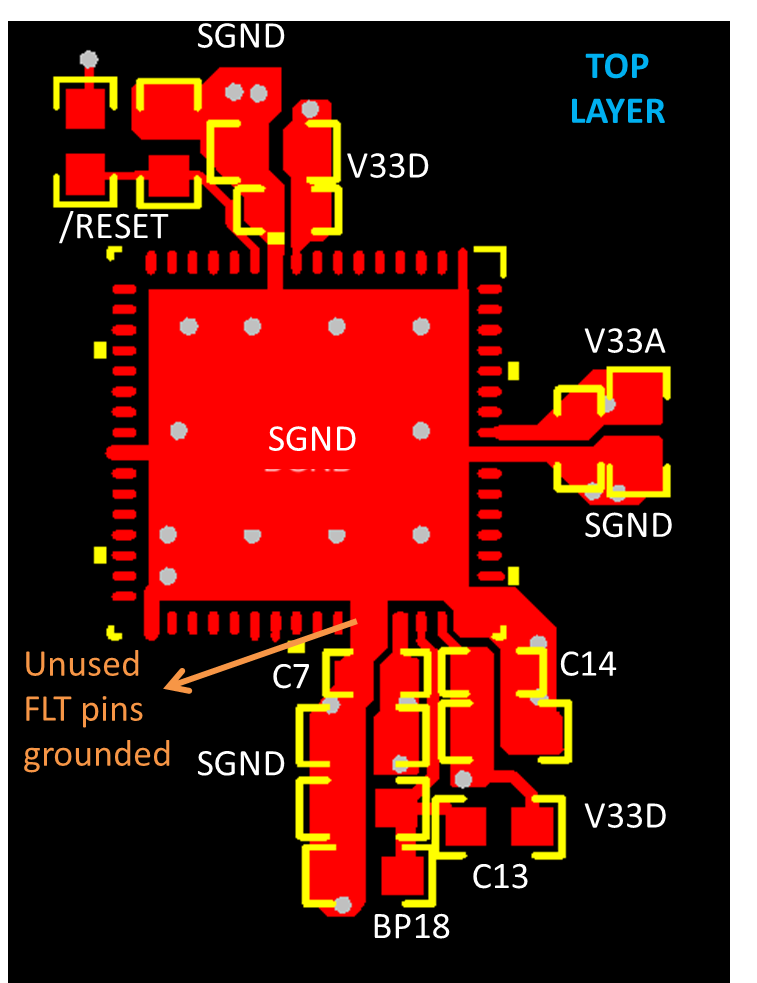
 Figure 12-13 UCD3138 and UCD3138064 64 Pin Layout
Top Layer
 Figure 12-14 64 Pin UCD3138 and UCD3138064 Layout
Internal SGND Layer
Figure 12-14 64 Pin UCD3138 and UCD3138064 Layout
Internal SGND LayerIf it is not possible to fit all the capacitors on the top layer, there is an alternative recommended layout with the BP18 capacitors located on the bottom layer, directly underneath the UCD.
 Figure 12-15 Alternative UCD3138 and UCD3138064
64 Pin Layout Top Layer
 Figure 12-16 Alternative 64 Pin UCD3138 and
UCD3138064 Layout Bottom Layer