JAJSP77A November 2019 – August 2020 BQ79600-Q1
PRODUCTION DATA
- 1 特長
- 2 アプリケーション
- 3 概要
- 4 Revision History
- 5 Pin Configuration and Functions
- 6 仕様
-
7 Detailed Description
- 7.1 Overview
- 7.2 Functional Block Diagram
- 7.3
Feature Description
- 7.3.1 Functional Modes and Power Supply
- 7.3.2 Communication
- 7.3.3 Fault Handling
- 7.3.4 INH/ Reverse Wakeup
- 7.3.5 Sniff Detector
- 7.3.6 Device Diagnostic
- 7.4 Device Functional Modes
- 7.5
Register Maps
- 7.5.1 Register Summary Table
- 7.5.2 Register: DIR0_ADDR
- 7.5.3 Register: DIR1_ADDR
- 7.5.4 Register: CONTROL1
- 7.5.5 Register: CONTROL2
- 7.5.6 Register: DIAG_CTRL
- 7.5.7 Register: DEV_CONF1
- 7.5.8 Register: DEV_CONF2
- 7.5.9 Register: TX_HOLD_OFF
- 7.5.10 Register: SLP_TIMEOUT
- 7.5.11 Register: COMM_TIMEOUT
- 7.5.12 Register: SPI_FIFO_UNLOCK
- 7.5.13 Register: FAULT_MSK
- 7.5.14 Register: FAULT_RST
- 7.5.15 Register: FAULT_SUMMARY
- 7.5.16 Register: FAULT_REG
- 7.5.17 Register: FAULT_SYS
- 7.5.18 Register: FAULT_PWR
- 7.5.19 Register: FAULT_COMM1
- 7.5.20 Register: FAULT_COMM2
- 7.5.21 Register: DEV_DIAG_STAT
- 7.5.22 Register: PARTID
- 7.5.23 Register: DIE_ID1
- 7.5.24 Register: DIE_ID2
- 7.5.25 Register: DIE_ID3
- 7.5.26 Register: DIE_ID4
- 7.5.27 Register: DIE_ID5
- 7.5.28 Register: DIE_ID6
- 7.5.29 Register: DIE_ID7
- 7.5.30 Register: DIE_ID8
- 7.5.31 Register: DIE_ID9
- 7.5.32 Register: DEBUG_CTRL_UNLOCK
- 7.5.33 Register: DEBUG_COMM_CTRL
- 7.5.34 Register: DEBUG_COMM_STAT
- 7.5.35 Register: DEBUG_SPI_PHY
- 7.5.36 Register: DEBUG_SPI_FRAME
- 7.5.37 Register: DEBUG_UART_FRAME
- 7.5.38 Register: DEBUG_COMH_PHY
- 7.5.39 Register: DEBUG_COMH_FRAME
- 7.5.40 Register: DEBUG_COML_PHY
- 7.5.41 Register: DEBUG_COML_FRAME
- 8 Application and Implementation
- 9 Power Supply Recommendations
- 10Layout
- 11Device and Documentation Support
- 12Mechanical, Packaging, and Orderable Information
7.3.2.1.2.3 Daisy Chain
Daisy chain is the interface (COMH/COML) communicating to stack devices. It is bi-directional and half duplex, and, therefore, has a transmitter (TX) and receiver (RX) on both COMH and COML interfaces, Figure 7-1. Signal going in and out of daisy chain port is taken care by the device. To use the device, host does not need to know daisy chain physical layer protocol (bit definition, byte definition and byte transferring). Host just needs to control SPI or UART port properly. Still, for user's information, daisy chain physical layer protocol is described below.
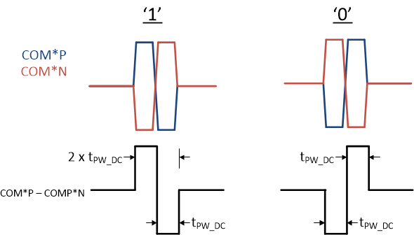
Daisy chain bit is transmitted between COM*P and COM*N in fully differential fashion, see Figure 7-19.
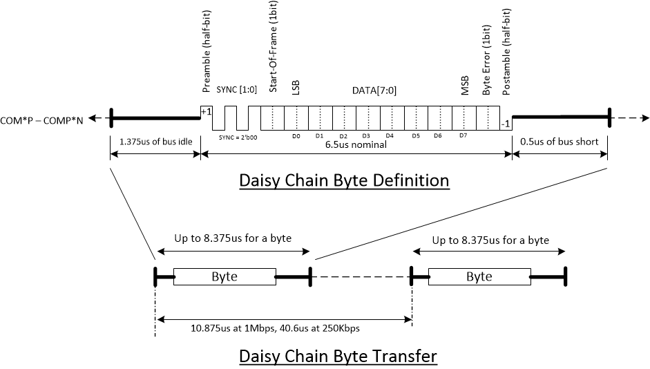
Daisy chain byte uses an asynchronous 13-bit byte-transfer protocol. The definition of each bit in the byte is defined in Table 7-6. Byte to byte transmission is captured in Figure 7-20.
 Figure 7-19 Daisy Chain Bit Definition
 Figure 7-20 Daisy Chain Byte/ Byte Transfer Definition
| BIT NAME | DESCRIPTION |
|---|---|
| Preamble (half-bit) | Indicates a start of byte transaction, signaling the receiver to start sampling. This half-bit and the following 2 SYNC bits are used for extra timing information. |
| SYNC[1:0] | Always 0b00. The SYNC bits are used for the digital to assess the timing and noise level on the byte, improving the detection of a '1' and '0' in a noisy environment. |
| Start-Of-Frame (1-bit) | The Start-Of-Frame (SOF) bit defines the byte as the INIT byte (initialization byte) in the frame, refer to Figure 7-8. Stack device needs this information in order to process the communication. |
| Data[7:0] | The actual 8-bit payload. |
| Byte Error BERR (1-bit) | For BQ79600-Q1, BERR is always ‘0’ in command frames sent to stack device. While in received response frames, if it is ‘1’, it indicates last device DEBUG_COM*_PHY[PERR] = 1. |
| Postamble (half-bit) | Indicates the end of byte transaction. |