JAJSPP1A April 2020 – September 2020 CC2640R2L
PRODUCTION DATA
- 1 特長
- 2 アプリケーション
- 3 概要
- 4 Functional Block Diagram
- 5 Revision History
- 6 Device Comparison
- 7 Terminal Configuration and Functions
-
8 Specifications
- 8.1 Absolute Maximum Ratings
- 8.2 ESD Ratings
- 8.3 Recommended Operating Conditions
- 8.4 Power Consumption Summary
- 8.5 General Characteristics
- 8.6 125-kbps Coded (Bluetooth 5) – RX
- 8.7 125-kbps Coded (Bluetooth 5) – TX
- 8.8 500-kbps Coded (Bluetooth 5) – RX
- 8.9 500-kbps Coded (Bluetooth 5) – TX
- 8.10 1-Mbps GFSK (Bluetooth low energy) – RX
- 8.11 1-Mbps GFSK (Bluetooth low energy) – TX
- 8.12 2-Mbps GFSK (Bluetooth 5) – RX
- 8.13 2-Mbps GFSK (Bluetooth 5) – TX
- 8.14 24-MHz Crystal Oscillator (XOSC_HF)
- 8.15 32.768-kHz Crystal Oscillator (XOSC_LF)
- 8.16 48-MHz RC Oscillator (RCOSC_HF)
- 8.17 32-kHz RC Oscillator (RCOSC_LF)
- 8.18 ADC Characteristics
- 8.19 Temperature Sensor
- 8.20 Battery Monitor
- 8.21 Synchronous Serial Interface (SSI)
- 8.22 DC Characteristics
- 8.23 Thermal Resistance Characteristics
- 8.24 Timing Requirements
- 8.25 Switching Characteristics
- 8.26 Typical Characteristics
- 9 Detailed Description
- 10Application, Implementation, and Layout
- 11Device and Documentation Support
- 12Mechanical, Packaging, and Orderable Information
パッケージ・オプション
メカニカル・データ(パッケージ|ピン)
サーマルパッド・メカニカル・データ
発注情報
10.1 Application Information
Very few external components are required for the operation of the CC2640R2L device. This section provides some general information about the various configuration options when using the CC2640R2L in an application, and then shows two examples of application circuits with schematics and layout. This is only a small selection of the many application circuit examples available as complete reference designs from the product folder on www.ti.com.
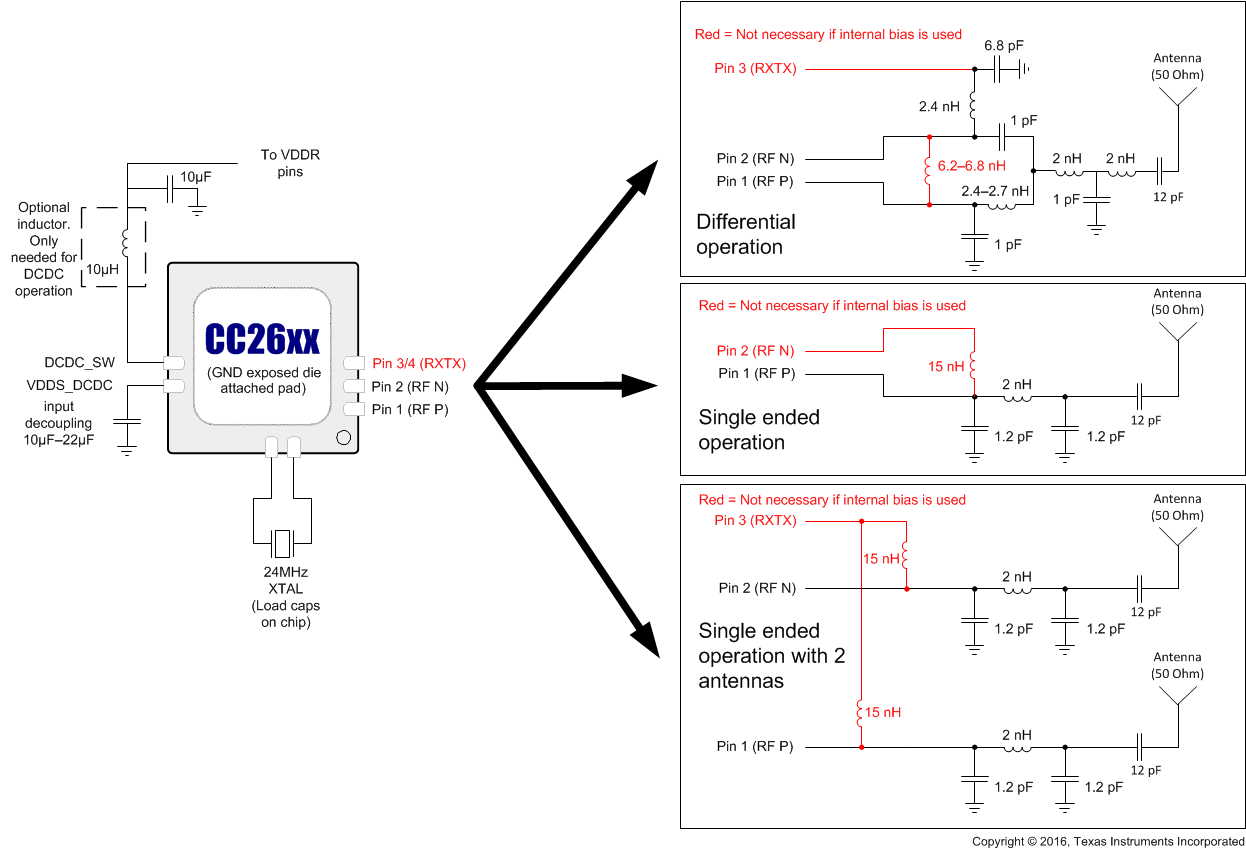
Figure 10-1 shows the various RF front-end configuration options. The RF front end can be used in differential- or single-ended configurations with the options of having internal or external biasing. These options allow for various trade-offs between cost, board space, and RF performance. Differential operation with external bias gives the best performance while single-ended operation with internal bias gives the least amount of external components and the lowest power consumption. Reference designs exist for each of these options.
 Figure 10-1 CC2640R2L Application Circuit
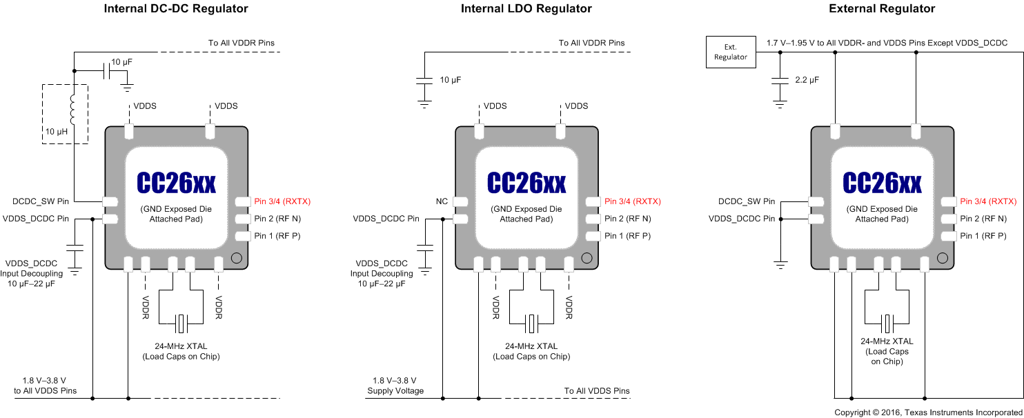
Figure 10-2 shows the various supply voltage configuration options. Not all power supply decoupling capacitors or digital I/Os are shown. Exact pin positions will vary between the different package options. For a detailed overview of power supply decoupling and wiring, see the TI reference designs and the CC26xx technical reference manual ().
 Figure 10-2 Supply Voltage Configurations