JAJSF86F April 2010 – April 2018 DLPC200
PRODUCTION DATA.
- 1 特長
- 2 アプリケーション
- 3 概要
- 4 改訂履歴
- 5 Pin Configuration and Functions
-
6 Specifications
- 6.1 Absolute Maximum Ratings
- 6.2 Handling Ratings
- 6.3 Recommended Operating Conditions
- 6.4 Thermal Information
- 6.5 I/O Electrical Characteristics
- 6.6 Video Input Pixel Interface Timing Requirements
- 6.7 I2C Interface Timing Requirements
- 6.8 USB Read Interface Timing Requirements
- 6.9 USB Write Interface Timing Requirements
- 6.10 SPI Slave Interface Timing Requirements
- 6.11 Parallel Flash Interface Timing Requirements
- 6.12 Serial Flash Interface Timing Requirements
- 6.13 Static RAM Interface Timing Requirements
- 6.14 DMD Interface Timing Requirements
- 6.15 DLPA200 Interface Timing Requirements
- 6.16 DDR2 SDR Memory Interface Timing Requirements
- 6.17 Video Input Pixel Interface – Image Sync and Blanking Requirements
- 7 Detailed Description
-
8 Application and Implementation
- 8.1 Application Information
- 8.2
Typical Application
- 8.2.1 Design Requirements
- 8.2.2
Detailed Design Procedure
- 8.2.2.1
DLPC200 System Interfaces
- 8.2.2.1.1 DLPC200 Master, I2C Interface for EDID Programming
- 8.2.2.1.2 USB Interface
- 8.2.2.1.3 Bus Protocol
- 8.2.2.1.4 SPI Slave Interface
- 8.2.2.1.5 Parallel Flash Memory Interface
- 8.2.2.1.6 Serial Flash Memory Interface
- 8.2.2.1.7 SRAM Interface
- 8.2.2.1.8 DDR2 SDR Memory Interface
- 8.2.2.1.9 Projector Image and Control Port Signals
- 8.2.2.1.10 SDRAM Memory
- 8.2.2.1
DLPC200 System Interfaces
- 8.2.3 Application Curve
- 9 Power Supply Recommendations
- 10Layout
- 11デバイスおよびドキュメントのサポート
- 12メカニカル、パッケージ、および注文情報
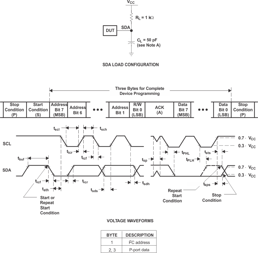
6.7 I2C Interface Timing Requirements
| PARAMETER | MIN | MAX | UNIT | ||
|---|---|---|---|---|---|
| ƒscl | I2C clock frequency | 0 | 400 | kHz | |
| tsch | I2C clock high time | 1 | ms | ||
| tscl | I2C clock low time | 1 | ms | ||
| tsp | I2C spike time | 20 | ns | ||
| tsds | I2C serial-data setup time | 100 | ns | ||
| tsdh | I2C serial-data hold time | 100 | ns | ||
| ticr | I2C input rise time | 100 | ns | ||
| tocf | I2C output fall time | 50 pF | 30 | 200 | ns |
| tbuf | I2C bus free time between stop and start conditions | 1.3 | ms | ||
| tsts | I2C start or repeat start condition setup | 1 | ms | ||
| tsth | I2C start or repeat start condition hold | 1 | ms | ||
| tsph | I2C stop condition setup | 1 | ms | ||
| tvd | Valid-data time | SCL low to SDA output valid | 1 | ms | |
| Valid-data time of ACK condition | ACK signal from SCL low to SDA (out) low | 1 | ms | ||
| tsch | I2C bus capacitive load | 0 | 100 | pF | |
 Figure 2. I2C Interface Load Circuit and Voltage Waveforms