JAJSF86F April 2010 – April 2018 DLPC200
PRODUCTION DATA.
- 1 特長
- 2 アプリケーション
- 3 概要
- 4 改訂履歴
- 5 Pin Configuration and Functions
-
6 Specifications
- 6.1 Absolute Maximum Ratings
- 6.2 Handling Ratings
- 6.3 Recommended Operating Conditions
- 6.4 Thermal Information
- 6.5 I/O Electrical Characteristics
- 6.6 Video Input Pixel Interface Timing Requirements
- 6.7 I2C Interface Timing Requirements
- 6.8 USB Read Interface Timing Requirements
- 6.9 USB Write Interface Timing Requirements
- 6.10 SPI Slave Interface Timing Requirements
- 6.11 Parallel Flash Interface Timing Requirements
- 6.12 Serial Flash Interface Timing Requirements
- 6.13 Static RAM Interface Timing Requirements
- 6.14 DMD Interface Timing Requirements
- 6.15 DLPA200 Interface Timing Requirements
- 6.16 DDR2 SDR Memory Interface Timing Requirements
- 6.17 Video Input Pixel Interface – Image Sync and Blanking Requirements
- 7 Detailed Description
-
8 Application and Implementation
- 8.1 Application Information
- 8.2
Typical Application
- 8.2.1 Design Requirements
- 8.2.2
Detailed Design Procedure
- 8.2.2.1
DLPC200 System Interfaces
- 8.2.2.1.1 DLPC200 Master, I2C Interface for EDID Programming
- 8.2.2.1.2 USB Interface
- 8.2.2.1.3 Bus Protocol
- 8.2.2.1.4 SPI Slave Interface
- 8.2.2.1.5 Parallel Flash Memory Interface
- 8.2.2.1.6 Serial Flash Memory Interface
- 8.2.2.1.7 SRAM Interface
- 8.2.2.1.8 DDR2 SDR Memory Interface
- 8.2.2.1.9 Projector Image and Control Port Signals
- 8.2.2.1.10 SDRAM Memory
- 8.2.2.1
DLPC200 System Interfaces
- 8.2.3 Application Curve
- 9 Power Supply Recommendations
- 10Layout
- 11デバイスおよびドキュメントのサポート
- 12メカニカル、パッケージ、および注文情報
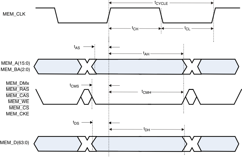
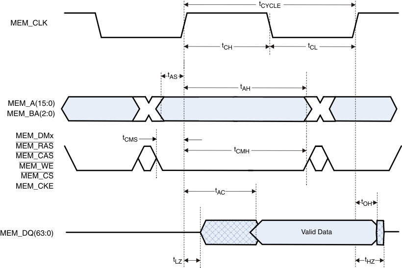
6.16 DDR2 SDR Memory Interface Timing Requirements
| PARAMETER | MIN | MAX | UNIT | |
|---|---|---|---|---|
| tCYCLE | Cycle time reference | 5 | 8 | ns |
| tCH | CK high pulse duration(1) | 2.4 | 4.16 | ns |
| tCL | CK low pulse duration(1) | 2.4 | 4.16 | ns |
| tCMS | Command setup | 200 | ps | |
| tCMH | Command hold | 275 | ps | |
| tAS | Address setup | 400 | ps | |
| tAH | Address hold | 400 | ps | |
| tDS | Write data setup | 1.5 | ns | |
| tDH | Write data hold | 1.5 | ns | |
| tAC | Read data access time | –450 | 450 | ps |
| tOH | Read data hold time | 340 | ps | |
| tLZ | Read data low-impedance time | –900 | 450 | ps |
| tHZ | Read data high-impedance time | 450 | ps | |
(1) Output setup/hold numbers already account for controller clock jitter. Only routing skew and memory setup/hold need be considered in system timing analysis.
 Figure 11. SDR Memory I/F Write Timing
 Figure 12. SDR Memory I/F Read Timing