JAJSFM2E April   2018  – September 2019 ISO1410 , ISO1412 , ISO1430 , ISO1432 , ISO1450 , ISO1452

UNLESS OTHERWISE NOTED, this document contains PRODUCTION DATA.  

  1. 特長
  2. アプリケーション
  3. 概要
    1.     簡略化されたアプリケーション回路図
  4. 改訂履歴
  5. 概要(続き)
  6. Device Options
  7. Pin Configuration and Functions
    1.     Pin Functions: Full-Duplex Device
    2.     Pin Functions: Half-Duplex Device
  8. Specifications
    1. 8.1  Absolute Maximum Ratings
    2. 8.2  ESD Ratings
    3. 8.3  Recommended Operating Conditions
    4. 8.4  Thermal Information
    5. 8.5  Power Ratings
    6. 8.6  Insulation Specifications
    7. 8.7  Safety-Related Certifications
    8. 8.8  Safety Limiting Values
    9. 8.9  Electrical Characteristics: Driver
    10. 8.10 Electrical Characteristics: Receiver
    11. 8.11 Supply Current Characteristics: Side 1 (ICC1)
    12. 8.12 Supply Current Characteristics: Side 2 (ICC2)
    13. 8.13 Switching Characteristics: Driver
    14. 8.14 Switching Characteristics: Receiver
    15. 8.15 Insulation Characteristics Curves
    16. 8.16 Typical Characteristics
  9. Parameter Measurement Information
  10. 10Detailed Description
    1. 10.1 Overview
    2. 10.2 Functional Block Diagram
    3. 10.3 Feature Description
      1. 10.3.1 Electromagnetic Compatibility (EMC) Considerations
      2. 10.3.2 Failsafe Receiver
      3. 10.3.3 Thermal Shutdown
      4. 10.3.4 Glitch-Free Power Up and Power Down
    4. 10.4 Device Functional Modes
      1. 10.4.1 Device I/O Schematics
  11. 11Application and Implementation
    1. 11.1 Application Information
    2. 11.2 Typical Application
      1. 11.2.1 Design Requirements
      2. 11.2.2 Detailed Design Procedure
        1. 11.2.2.1 Data Rate and Bus Length
        2. 11.2.2.2 Stub Length
        3. 11.2.2.3 Bus Loading
      3. 11.2.3 Application Curves
        1. 11.2.3.1 Insulation Lifetime
  12. 12Power Supply Recommendations
  13. 13Layout
    1. 13.1 Layout Guidelines
      1. 13.1.1 PCB Material
    2. 13.2 Layout Example
  14. 14デバイスおよびドキュメントのサポート
    1. 14.1 ドキュメントのサポート
      1. 14.1.1 関連資料
    2. 14.2 関連リンク
    3. 14.3 ドキュメントの更新通知を受け取る方法
    4. 14.4 コミュニティ・リソース
    5. 14.5 商標
    6. 14.6 静電気放電に関する注意事項
    7. 14.7 Glossary
  15. 15メカニカル、パッケージ、および注文情報

パッケージ・オプション

デバイスごとのパッケージ図は、PDF版データシートをご参照ください。

メカニカル・データ(パッケージ|ピン)
  • DW|16
サーマルパッド・メカニカル・データ
発注情報

Parameter Measurement Information

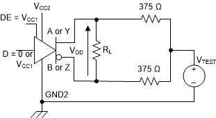
ISO1450 ISO1452 ISO1410 ISO1412 ISO1430 ISO1432 iso14xx-driver-voltages.gifFigure 35. Driver Voltages
ISO1450 ISO1452 ISO1410 ISO1412 ISO1430 ISO1432 iso14xx_driver_voltages.gif
RL = 100 Ω for RS422, RL = 54 Ω for RS-485
Figure 36. Driver Voltages
ISO1450 ISO1452 ISO1410 ISO1412 ISO1430 ISO1432 iso14xx_driver_switching_specifications.gif
CL includes fixture and instrumentation capacitance.
Figure 37. Driver Switching Specifications
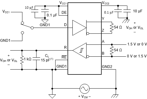
ISO1450 ISO1452 ISO1410 ISO1412 ISO1430 ISO1432 iso14xx_common-mode-transient-imunity-full-duplex-circuit.gif
Includes probe and fixture capacitance.
Figure 38. Common Mode Transient Immunity (CMTI)—Full Duplex
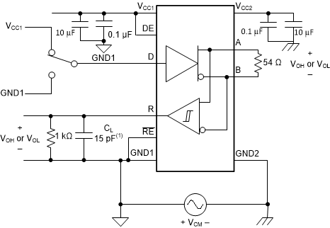
ISO1450 ISO1452 ISO1410 ISO1412 ISO1430 ISO1432 iso14xx_common-mode-transient-imunity-half-duplex-circuit.gif
Includes probe and fixture capacitance.
Figure 39. Common Mode Transient Immunity (CMTI)—Half Duplex
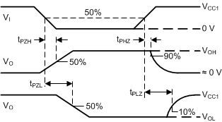
ISO1450 ISO1452 ISO1410 ISO1412 ISO1430 ISO1432 iso14xx_driver_enable_disable_times.gif
CL includes fixture and instrumentation capacitance
Figure 40. Driver Enable and Disable Times
ISO1450 ISO1452 ISO1410 ISO1412 ISO1430 ISO1432 iso14xx_driver_enable_disable_times_vcc2.gifFigure 41. Driver Enable and Disable Times
ISO1450 ISO1452 ISO1410 ISO1412 ISO1430 ISO1432 iso14xx_receiver_switching_specs.gif
CL includes fixture and instrumentation capacitance.
Figure 42. Receiver Switching Specifications
ISO1450 ISO1452 ISO1410 ISO1412 ISO1430 ISO1432 iso14xx-receiver-enable-and-disable_times-1.gifFigure 43. Receiver Enable and Disable Times
ISO1450 ISO1452 ISO1410 ISO1412 ISO1430 ISO1432 iso14xx-receiver-enable-and-disable_times-2.gifFigure 44. Receiver Enable and Disable Times
ISO1450 ISO1452 ISO1410 ISO1412 ISO1430 ISO1432 iso14xx_short_circuit_current_limiting.gif
The driver should not sustain any damage with this configuration.
Figure 45. Short-Circuit Current Limiting