JAJSFM2E April 2018 – September 2019 ISO1410 , ISO1412 , ISO1430 , ISO1432 , ISO1450 , ISO1452
UNLESS OTHERWISE NOTED, this document contains PRODUCTION DATA.
- 1 特長
- 2 アプリケーション
- 3 概要
- 4 改訂履歴
- 5 概要(続き)
- 6 Device Options
- 7 Pin Configuration and Functions
-
8 Specifications
- 8.1 Absolute Maximum Ratings
- 8.2 ESD Ratings
- 8.3 Recommended Operating Conditions
- 8.4 Thermal Information
- 8.5 Power Ratings
- 8.6 Insulation Specifications
- 8.7 Safety-Related Certifications
- 8.8 Safety Limiting Values
- 8.9 Electrical Characteristics: Driver
- 8.10 Electrical Characteristics: Receiver
- 8.11 Supply Current Characteristics: Side 1 (ICC1)
- 8.12 Supply Current Characteristics: Side 2 (ICC2)
- 8.13 Switching Characteristics: Driver
- 8.14 Switching Characteristics: Receiver
- 8.15 Insulation Characteristics Curves
- 8.16 Typical Characteristics
- 9 Parameter Measurement Information
- 10Detailed Description
- 11Application and Implementation
- 12Power Supply Recommendations
- 13Layout
- 14デバイスおよびドキュメントのサポート
- 15メカニカル、パッケージ、および注文情報
パッケージ・オプション
デバイスごとのパッケージ図は、PDF版データシートをご参照ください。
メカニカル・データ(パッケージ|ピン)
- DW|16
サーマルパッド・メカニカル・データ
- DW|16
発注情報
10.3.2 Failsafe Receiver
The differential receiver of the ISO14xx devices has failsafe protection from invalid bus states caused by:
- Open bus conditions such as a broken cable or a disconnected connector
- Shorted bus conditions such as insulation breakdown of a cable that shorts the twisted-pair
- Idle bus conditions that occur when no driver on the bus is actively driving
The differential input of the RS-485 receiver is 0 in any of these conditions for a terminated transmission line. The receiver outputs a failsafe logic-high state so that the output of the receiver is not indeterminate.
The receiver thresholds are offset in the receiver failsafe protection so that the indeterminate range of the does not include a 0 V differential. The receiver output must generate a logic high when the differential input (VID) is greater than 200 mV to comply with the RS-485 standard. The receiver output must also generate a output a logic low when VID is less than –200 mV to comply with the RS-485 standard. The receiver parameters that determine the failsafe performance are VTH+, VTH–, and VHYS. Differential signals less than –200 mV always cause a low receiver output as shown in the Electrical Characteristics table. Differential signals greater than 200 mV always cause a high receiver output. A differential input signal that is near zero is still greater than the VTH+ threshold which makes the receiver output logic high. The receiver output goes to a low state only when the differential input decreases by VHYS to less than VTH+.
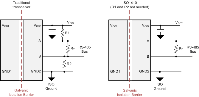
The internal failsafe biasing feature removes the need for the two external resistors that are typically required with traditional isolated RS-485 transceivers as shown in Figure 48.
 Figure 48. Failsafe Transceiver