JAJSAU5C August 2008 – November 2015 LMV831 , LMV832 , LMV834
PRODUCTION DATA.
7.3.2 EMIRR
With the increase of RF transmitting devices in the world, the electromagnetic interference (EMI) between those devices and other equipment becomes a bigger challenge. The LMV831, LMV832, and LMV834 are EMI-hardened operational amplifiers which are specifically designed to overcome electromagnetic interference. Along with EMI-hardened operational amplifiers, the EMIRR parameter is introduced to unambiguously specify the EMI performance of an operational amplifier. This section presents an overview of EMIRR. A detailed description on this specification for EMI-hardened operational amplifiers can be found in AN-1698 (SNOA497).
The dimensions of an operational amplifier IC are relatively small compared to the wavelength of the disturbing RF signals. As a result the operational amplifier itself will hardly receive any disturbances. The RF signals interfering with the operational amplifier are dominantly received by the PCB and wiring connected to the operational amplifier. As a result the RF signals on the pins of the operational amplifier can be represented by voltages and currents. This representation significantly simplifies the unambiguous measurement and specification of the EMI performance of an operational amplifier.
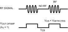
RF signals interfere with operational amplifiers through the non-linearity of the operational amplifier circuitry. This non-linearity results in the detection of the so called out-of-band signals. The obtained effect is that the amplitude modulation of the out-of-band signal is downconverted into the base band. This base band can easily overlap with the band of the operational amplifier circuit. As an example Figure 43 depicts a typical output signal of a unity-gain connected operational amplifier in the presence of an interfering RF signal. Clearly the output voltage varies in the rhythm of the on-off keying of the RF carrier.
 Figure 43. Offset Voltage Variation Due to an Interfering RF Signal