JAJSAU5C August   2008  – November 2015 LMV831 , LMV832 , LMV834

PRODUCTION DATA.  

  1. 特長
  2. アプリケーション
  3. 概要
    1.     Device Images
      1.      代表的なアプリケーション
  4. 改訂履歴
  5. Pin Configuration and Functions
    1.     Pin Functions
  6. Specifications
    1. 6.1 Absolute Maximum Ratings
    2. 6.2 ESD Ratings
    3. 6.3 Recommended Operating Conditions
    4. 6.4 Thermal Information
    5. 6.5 Electrical Characteristics, 3.3 V
    6. 6.6 Electrical Characteristics, 5 V
    7. 6.7 Typical Characteristics
  7. Detailed Description
    1. 7.1 Overview
    2. 7.2 Functional Block Diagram
    3. 7.3 Feature Description
      1. 7.3.1 Input Characteristics
      2. 7.3.2 EMIRR
      3. 7.3.3 EMIRR Definition
        1. 7.3.3.1 Coupling an RF Signal to the IN+ Pin
        2. 7.3.3.2 Cell Phone Call
    4. 7.4 Device Functional Modes
      1. 7.4.1 Output Characteristics
      2. 7.4.2 CMRR Measurement
  8. Application and Implementation
    1. 8.1 Application Information
    2. 8.2 Typical Application
      1. 8.2.1 Design Requirements
      2. 8.2.2 Detailed Design Procedure
      3. 8.2.3 Application Curve
  9. Power Supply Recommendations
  10. 10Layout
    1. 10.1 Layout Guidelines
    2. 10.2 Layout Example
  11. 11デバイスおよびドキュメントのサポート
    1. 11.1 デバイス・サポート
      1. 11.1.1 開発サポート
    2. 11.2 ドキュメントのサポート
      1. 11.2.1 関連資料
    3. 11.3 関連リンク
    4. 11.4 コミュニティ・リソース
    5. 11.5 商標
    6. 11.6 静電気放電に関する注意事項
    7. 11.7 Glossary
  12. 12メカニカル、パッケージ、および注文情報

パッケージ・オプション

メカニカル・データ(パッケージ|ピン)
サーマルパッド・メカニカル・データ
発注情報

Pin Configuration and Functions

DCK Package
5-Pin SC70
Top View
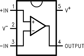
LMV831 LMV832 LMV834 30024102.png
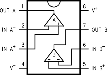
DGK Package
8-Pin VSSOP
Top View
LMV831 LMV832 LMV834 30024103.png
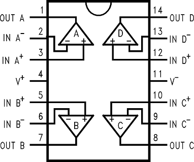
PW Package
14-Pin TSSOP
Top View
LMV831 LMV832 LMV834 30024104.png

Pin Functions

PIN TYPE DESCRIPTION
NAME SC70 VSSOP TSSOP
IN+ 1 I Noninverting Input
IN– 3 I Inverting Input
IN A+ 3 3 I Noninverting Input, Channel A
IN A 2 2 I Inverting Input, Channel A
IN B+ 5 5 I Noninverting Input, Channel B
IN B 6 6 I Inverting Input, Channel B
IN C+ 10 I Noninverting Input, Channel C
IN C 9 I Inverting Input, Channel C
IN D+ 12 I Noninverting Input, Channel D
IN D 13 I Inverting Input, Channel D
OUT A 1 1 O Output, Channel A
OUT B 7 7 O Output, Channel B
OUT C 8 O Output, Channel C
OUT D 14 O Output, Channel D
OUTPUT 4 O Output
V+ 5 8 4 P Positive (highest) Power Supply
V 2 4 11 P Negative (lowest) Power Supply