JAJSAU5C August 2008 – November 2015 LMV831 , LMV832 , LMV834
PRODUCTION DATA.
7.3.3.1 Coupling an RF Signal to the IN+ Pin
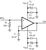
Each of the operational amplifier pins can be tested separately on EMIRR. In this section, the measurements on the IN+ pin (which, based on symmetry considerations, also apply to the IN– pin) are discussed. In AN-1698 (SNOA497) the other pins of the operational amplifier are treated as well. For testing the IN+ pin the operational amplifier is connected in the unity gain configuration. Applying the RF signal is straightforward as it can be connected directly to the IN+ pin. As a result the RF signal path has a minimum of components that might affect the RF signal level at the pin. The circuit diagram is shown in Figure 44. The PCB trace from RFIN to the IN+ pin should be a 50-Ω stripline in order to match the RF impedance of the cabling and the RF generator. On the PCB a 50-Ω termination is used. This 50-Ω resistor is also used to set the bias level of the IN+ pin to ground level. For determining the EMIRR, two measurements are needed: one is measuring the DC output level when the RF signal is off; and the other is measuring the DC output level when the RF signal is switched on. The difference of the two DC levels is the output voltage shift as a result of the RF signal. As the operational amplifier is in the unity-gain configuration, the input referred offset voltage shift corresponds one-to-one to the measured output voltage shift.
 Figure 44. Circuit for Coupling the RF Signal to IN+