JAJSHQ8D July 2019 – July 2021 TPS25832-Q1 , TPS25833-Q1
PRODUCTION DATA
- 1 特長
- 2 アプリケーション
- 3 概要
- 4 Revision History
- 5 概要 (続き)
- 6 Device Comparison Table
- 7 Pin Configuration and Functions
- 8 Specifications
- 9 Parameter Measurement Information
-
10Detailed Description
- 10.1 Overview
- 10.2 Functional Block Diagram
- 10.3
Feature Description
- 10.3.1 Buck Regulator
- 10.3.2 Enable/UVLO and Start-up
- 10.3.3 RT/SYNC
- 10.3.4 Spread-Spectrum Operation
- 10.3.5 VCC, VCC_UVLO
- 10.3.6 Minimum ON-time, Minimum OFF-time
- 10.3.7 Internal Compensation
- 10.3.8 Bootstrap Voltage (BOOT)
- 10.3.9 RSNS, RSET, RILIMIT, and RIMON
- 10.3.10 Overcurrent and Short Circuit Protection
- 10.3.11 IEC and Overvoltage Protection
- 10.3.12 Cable Compensation
- 10.3.13 USB Port Control
- 10.3.14 FAULT Response
- 10.3.15 USB Specification Overview
- 10.3.16 USB Type-C® Basics
- 10.3.17 Device Power Pins (IN, CSN/OUT, and PGND)
- 10.3.18 Thermal Shutdown
- 10.3.19 Power Wake
- 10.3.20 Thermal Sensing with NTC (TPS25833-Q1)
- 10.4
Device Functional Modes
- 10.4.1 Shutdown Mode
- 10.4.2 Standby Mode
- 10.4.3 Active Mode
- 10.4.4 Device Truth Table (TT)
- 10.4.5 USB Port Operating Modes
- 10.4.6 High-Bandwidth Data-Line Switches (TPS25832-Q1 Only)
-
11Application and Implementation
- 11.1 Application Information
- 11.2
Typical Application
- 11.2.1 Design Requirements
- 11.2.2
Detailed Design Procedure
- 11.2.2.1 Output Voltage
- 11.2.2.2 Switching Frequency
- 11.2.2.3 Inductor Selection
- 11.2.2.4 Output Capacitor Selection
- 11.2.2.5 Input Capacitor Selection
- 11.2.2.6 Bootstrap Capacitor Selection
- 11.2.2.7 VCC Capacitor Selection
- 11.2.2.8 Enable and Under Voltage Lockout Set-Point
- 11.2.2.9 Current Limit Set-Point
- 11.2.2.10 Cable Compensation Set-Point
- 11.2.2.11 LD_DET, POL, and FAULT Resistor Selection
- 11.2.3 Application Curves
- 12Power Supply Recommendations
- 13Layout
- 14Device and Documentation Support
- 15Mechanical, Packaging, and Orderable Information
パッケージ・オプション
メカニカル・データ(パッケージ|ピン)
- RHB|32
サーマルパッド・メカニカル・データ
- RHB|32
発注情報
7 Pin Configuration and Functions
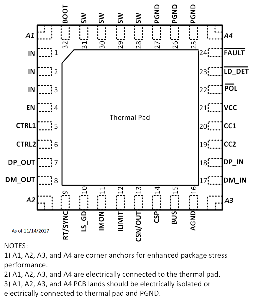
 Figure 7-1 TPS25832QWRHBRQ1 Package32-Pin (VQFN)Top View
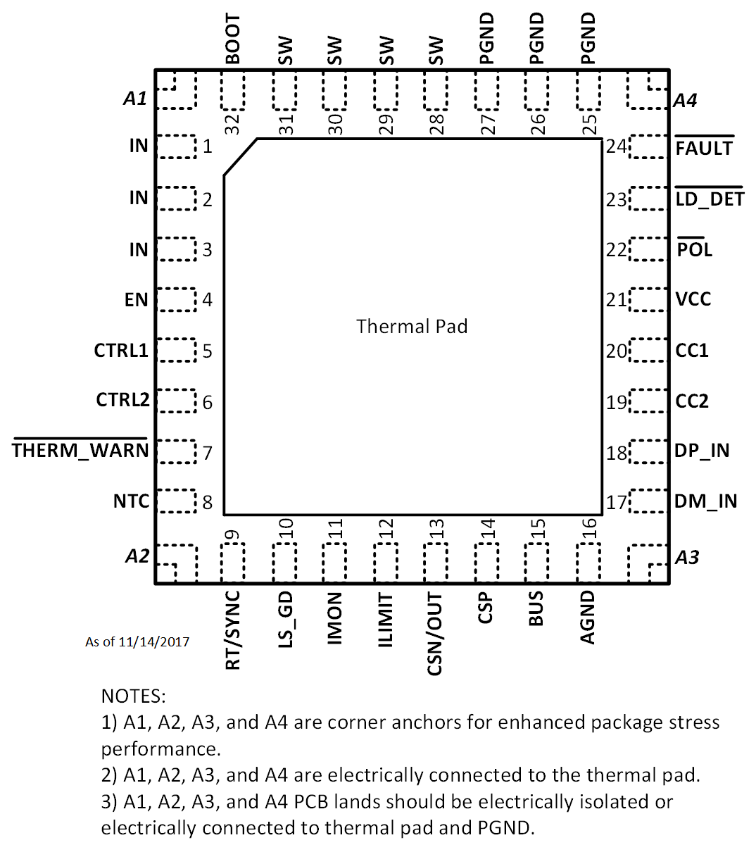
 Figure 7-3 TPS25832QCWRHBRQ1 Package32-Pin (VQFN)Top View
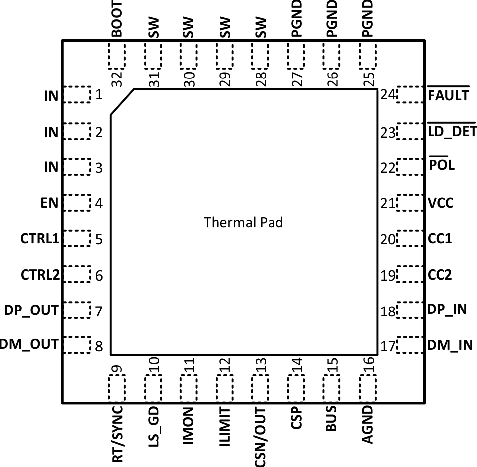
 Figure 7-2 TPS25833QWRHBRQ1 Package32-Pin (VQFN)Top View
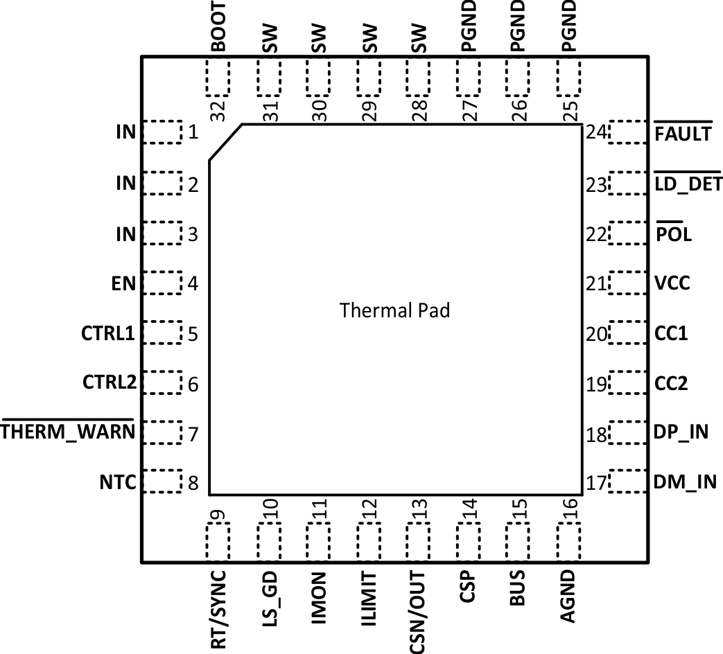
 Figure 7-4 TPS25833QCWRHBRQ1 Package32-Pin (VQFN)Top View
Table 7-1 Pin Functions
| NAME | 832-Q1 NO. |
833-Q1 NO. |
TYPE (1) | I/O | DESCRIPTION |
|---|---|---|---|---|---|
| AGND | 16 | 16 | G | – | Analog ground terminal. Ground reference for internal references and logic. All electrical parameters are measured with respect to this pin. Connect to system ground on PCB. |
| BOOT | 32 | 32 | P | Boot-strap capacitor connection for HS FET driver. Connect a high quality 100-nF capacitor from this pin to the SW pin. | |
| BUS | 15 | 15 | A | I | VBUS discharge input. Connect to VBUS on USB Connector. |
| CC1 | 20 | 20 | A | I/O | Analog input/output. Connect to Type-C CC1 pin. |
| CC2 | 19 | 19 | A | I/O | Analog input/output. Connect to Type-C CC2 pin. |
| CSN/OUT | 13 | 13 | A | I | Negative input of current sense amplifier, also buck output for internal voltage regulation. |
| CSP | 14 | 14 | A | I | Positive input of current sense amplifier. |
| CTRL1 | 5 | 5 | A | I | Logic-level control inputs for device/system configuration (see Table 10-10). |
| CTRL2 | 6 | 6 | A | I | Logic-level control inputs for device/system configuration (see Table 10-10). |
| DM_IN | 17 | 17 | A | DM data line. Connect to USB connector. | |
| DM_OUT | 8 | – | A | DM data line. Connect to USB host controller. | |
| DP_IN | 18 | 18 | A | DP data line. Connect to USB connector. | |
| DP_OUT | 7 | – | A | DP data line. Connect to USB host controller. | |
| EN/UVLO | 4 | 4 | A | Enable pin. Do not float. High = on, Low = off. Can be tied to VIN. Precision enable input allows adjustable UVLO by external resistor divider. | |
| FAULT | 24 | 24 | A | O | Active LOW open-drain output. Asserted during fault conditions (see Table 10-4). |
| ILIMIT | 12 | 12 | A | External resistor used to set the current-limit threshold (see Table 10-2). | |
| IMON | 11 | 11 | A | External resistor used to set the max cable comp voltage at full load current. | |
| IN | 1, 2, 3 | 1, 2, 3 | P | I | Input Supply to regulator. Connect a high-quality bypass capacitor(s) directly to this pin and PGND. |
| LD_DET | 23 | 23 | A | O | Active LOW open-drain output. Asserted when a Type-C UFP is identified on the CC lines. |
| LS_GD | 10 | 10 | A | External NMOS gate driver. For TPS25832-Q1, LS_GD pin must be pulled up through a 2.2-kΩ resistor under average current limit mode.(see Current Limit Setting using RILIMIT). | |
| NTC | – | 8 | I | Input for negative temperature coefficient resistor divider. Use to monitor external PCB temperature (see Thermal Sensing with NTC (TPS25833-Q1)). | |
| PGND | 25, 26, 27 | 25, 26, 27 | G | – | Power ground terminal. Connect to system ground and AGND. Connect to bypass capacitor with short wide traces. |
| POL | 22 | 22 | A | O | Active LOW open-drain output. Signals which Type-C CC pin is connected to the CC line. This gives cable orientation information needed to mux the super speed lines. Asserted when the CC2 pin is connected to the CC line in the cable. |
| RT/SYNC | 9 | 9 | A | Resistor Timing or External Clock input. An internal amplifier holds this terminal at a fixed voltage when using an external resistor to ground to set the switching frequency. If the terminal is pulled above the PLL upper threshold, a mode change occurs and the terminal becomes a synchronization input. The internal amplifier is disabled and the terminal is a high impedance clock input to the internal PLL. If clocking edges stop, the internal amplifier is re-enabled and the operating mode returns to resistor frequency programming. | |
| SW | 28, 29, 30, 31 | 28, 29, 30, 31 | P | Switching output of the regulator. Internally connected to source of the HS FET and drain of the LS FET. Connect to power inductor. | |
| THERM_WARN | – | 7 | A | O | Active LOW open-drain output. Asserted when voltage at the NTC pin increases above the thermal warning threshold. |
| VCC | 21 | 21 | P | Output of internal bias supply. Used as supply to internal control circuits. Connect a high quality 2.2-µF capacitor from this pin to GND. |
(1) A = Analog, P = Power, G = Ground.