JAJSIN7 February 2020 TPS59632-Q1
PRODUCTION DATA.
- 1 特長
- 2 アプリケーション
- 3 概要
- 4 改訂履歴
- 5 Pin Configuration and Functions
- 6 Specifications
-
7 Detailed Description
- 7.1 Overview
- 7.2 Functional Block Diagram
- 7.3
Feature Description
- 7.3.1 PWM Operation
- 7.3.2 Current Sensing
- 7.3.3 Load-line (Droop)
- 7.3.4 Load Transients
- 7.3.5 Overshoot Reduction (OSR)
- 7.3.6 Undershoot Reduction (USR)
- 7.3.7 Autobalance Current Sharing
- 7.3.8 PWM And SKIP Signals
- 7.3.9 Bias Power (V5A, VDD, And VINTF) UVLO
- 7.3.10 Start-Up Sequence
- 7.3.11 Power Good Operation
- 7.3.12 Analog Current Monitor, IMON, And Corresponding Digital Output Current
- 7.3.13 Fault Behavior
- 7.3.14 Output Under Voltage Protection (UVP)
- 7.3.15 Output Over Voltage Protection (OVP)
- 7.3.16 Over Current Protection (OCP)
- 7.3.17 Over Current Warning
- 7.3.18 Input Voltage Limits
- 7.3.19 VID Table
- 7.4 User Selections
- 7.5 I2C Interface Operation
- 7.6 I2C Register Maps
-
8 Applications and Implementation
- 8.1 Application Information
- 8.2
Typical Application
- 8.2.1
3-Phase D-CAP+™, Step-Down Application
- 8.2.1.1 Design Requirements
- 8.2.1.2
Detailed Design Procedure
- 8.2.1.2.1 Step 1: Select Switching Frequency
- 8.2.1.2.2 Step 2: Set The Slew Rate
- 8.2.1.2.3 Step 3: Set The I2C Address
- 8.2.1.2.4 Step 4: Determine Inductor Value And Choose Inductor
- 8.2.1.2.5 Step 5: Current Sensing Resistance
- 8.2.1.2.6 Step 6: Select Over Current Protection (OCP) Setting
- 8.2.1.2.7 Step 7: Current Monitor (IMON) Setting
- 8.2.1.2.8 Step 8: Set the Load-Line Slope
- 8.2.1.2.9 Step 9: Voltage Feedback Resistor Calculation
- 8.2.1.2.10 Step 10: Ramp Compensation Selection
- 8.2.1.2.11 Step 11 Overshoot Reduction (OSR) selection
- 8.2.1.2.12 Step 12: Undershoot Reduction (USR) selection
- 8.2.1.2.13 Step 13: Loop Compensation
- 8.2.1.3 Application Performance Plots
- 8.2.1
3-Phase D-CAP+™, Step-Down Application
- 9 Power Supply Recommendations
- 10Layout
- 11デバイスおよびドキュメントのサポート
- 12メカニカル、パッケージ、および注文情報
6.8 Typical Characteristics
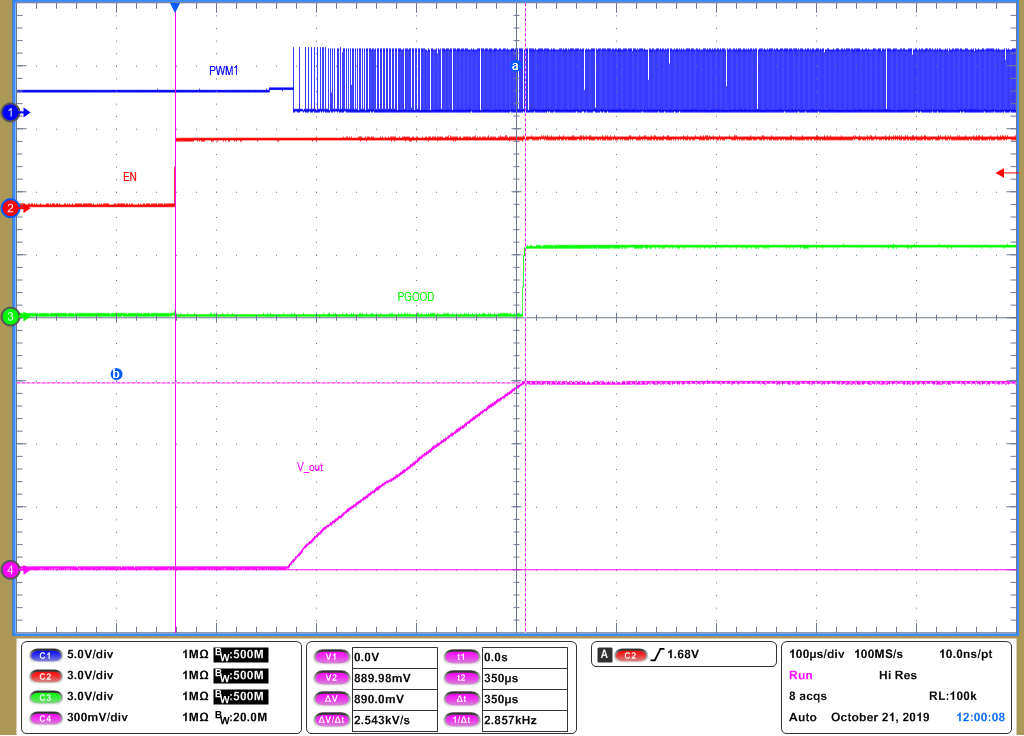 Figure 1. 3-phase start up behavior showing EN input and PGOOD output. Input Voltage = 5V, Load current = 10A.
 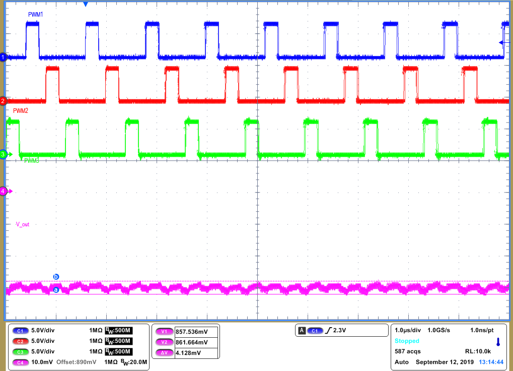 Figure 3. 3-phase switching ripple at Input Voltage = 5 V, Load current = 50A, Switching Frequency = 800kHz. Persistence mode.
 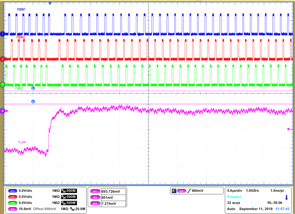 Figure 5. Load transient with a droop of 0.6mΩ load-line slope. Load transient = 36A to 0A. Single mode.
 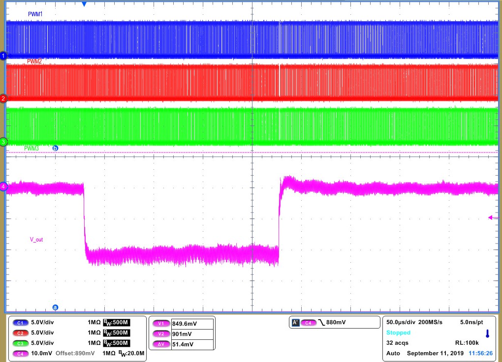 Figure 7. Load transient with a droop of 0.6mΩ load-line slope. Load transient = 0A to 36A. Persistence mode
 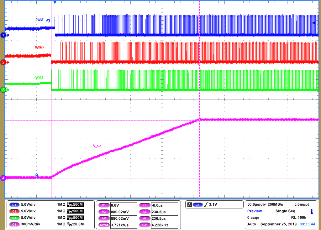 Figure 2. 3-phase start up behavior showing switching at startup. Input Voltage = 5V, Load current = 10A.
 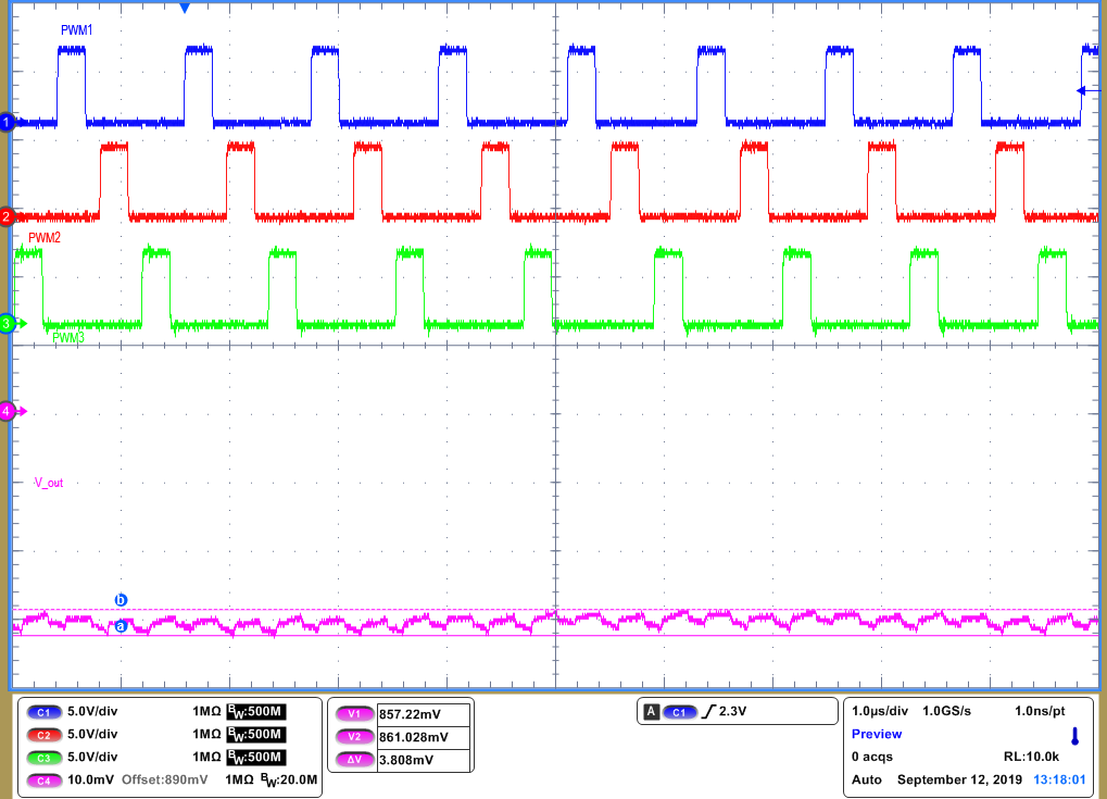 Figure 4. 3-phase switching ripple at Input Voltage = 5 V, Load current = 50A, Switching Frequency = 800kHz. Single mode.
 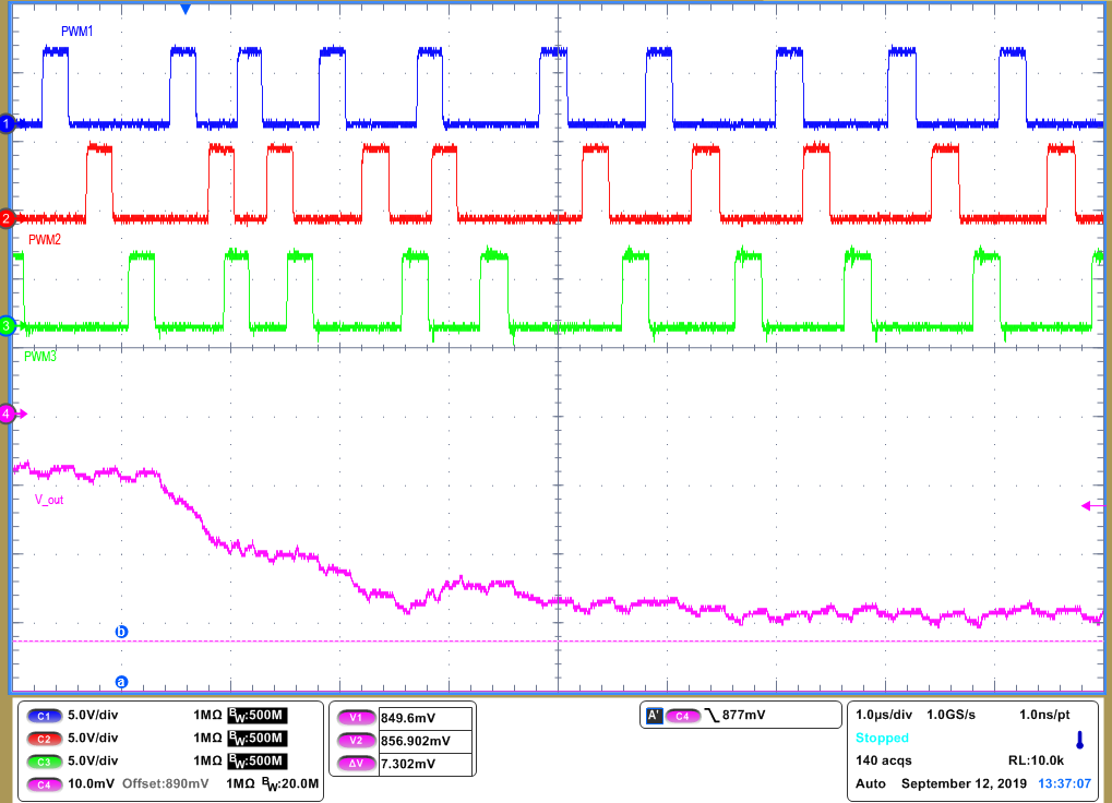 Figure 6. Load transient with a droop of 0.6mΩ load-line slope. Load transient = 14A to 50A. Single mode.
 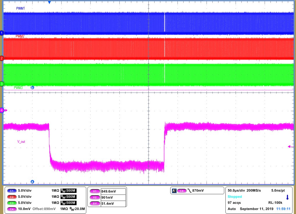 Figure 8. Load transient with a droop of 0.6mΩ load-line slope. Load transient = 14A to 50A. Persistence mode