JAJSIN7 February 2020 TPS59632-Q1
PRODUCTION DATA.
- 1 特長
- 2 アプリケーション
- 3 概要
- 4 改訂履歴
- 5 Pin Configuration and Functions
- 6 Specifications
-
7 Detailed Description
- 7.1 Overview
- 7.2 Functional Block Diagram
- 7.3
Feature Description
- 7.3.1 PWM Operation
- 7.3.2 Current Sensing
- 7.3.3 Load-line (Droop)
- 7.3.4 Load Transients
- 7.3.5 Overshoot Reduction (OSR)
- 7.3.6 Undershoot Reduction (USR)
- 7.3.7 Autobalance Current Sharing
- 7.3.8 PWM And SKIP Signals
- 7.3.9 Bias Power (V5A, VDD, And VINTF) UVLO
- 7.3.10 Start-Up Sequence
- 7.3.11 Power Good Operation
- 7.3.12 Analog Current Monitor, IMON, And Corresponding Digital Output Current
- 7.3.13 Fault Behavior
- 7.3.14 Output Under Voltage Protection (UVP)
- 7.3.15 Output Over Voltage Protection (OVP)
- 7.3.16 Over Current Protection (OCP)
- 7.3.17 Over Current Warning
- 7.3.18 Input Voltage Limits
- 7.3.19 VID Table
- 7.4 User Selections
- 7.5 I2C Interface Operation
- 7.6 I2C Register Maps
-
8 Applications and Implementation
- 8.1 Application Information
- 8.2
Typical Application
- 8.2.1
3-Phase D-CAP+™, Step-Down Application
- 8.2.1.1 Design Requirements
- 8.2.1.2
Detailed Design Procedure
- 8.2.1.2.1 Step 1: Select Switching Frequency
- 8.2.1.2.2 Step 2: Set The Slew Rate
- 8.2.1.2.3 Step 3: Set The I2C Address
- 8.2.1.2.4 Step 4: Determine Inductor Value And Choose Inductor
- 8.2.1.2.5 Step 5: Current Sensing Resistance
- 8.2.1.2.6 Step 6: Select Over Current Protection (OCP) Setting
- 8.2.1.2.7 Step 7: Current Monitor (IMON) Setting
- 8.2.1.2.8 Step 8: Set the Load-Line Slope
- 8.2.1.2.9 Step 9: Voltage Feedback Resistor Calculation
- 8.2.1.2.10 Step 10: Ramp Compensation Selection
- 8.2.1.2.11 Step 11 Overshoot Reduction (OSR) selection
- 8.2.1.2.12 Step 12: Undershoot Reduction (USR) selection
- 8.2.1.2.13 Step 13: Loop Compensation
- 8.2.1.3 Application Performance Plots
- 8.2.1
3-Phase D-CAP+™, Step-Down Application
- 9 Power Supply Recommendations
- 10Layout
- 11デバイスおよびドキュメントのサポート
- 12メカニカル、パッケージ、および注文情報
7.3.11 Power Good Operation
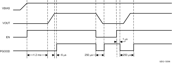
PGOOD is an open-drain output pin that is designed to be pulled-up with an external resistor to a voltage 3.6 V or less. Normal PGOOD operation (exclusive of activation of any faults) is shown in Figure 16. On initial power-up PGOOD happens within 6 µs of the DAC reaching its target value. When EN is brought low, PGOOD is also brought low for 250 µs, then is allowed to float. The TPS59632-Q1 device pulls down the PGOOD signal when the EN signal subsequently goes high and returns high again within 6 µs of the end of the DAC ramp. The delay period between EN going high and PGOOD going low in this case is less than 1 µs. Figure 16 shows the power good operation at initial start-up and with falling and rising EN.
For applications where it is undesirable to have PGOOD high when EN is low, an alternate method of pulling up the open-drain PGOOD signal is possible. In this method, the PGOOD is pulled up to EN logic signal. This ensures that the PGOOD is low when EN goes low.
 Figure 16. Power Good Operation