JAJSNJ1H May 2013 – December 2021 TPS65310A-Q1
PRODUCTION DATA
- 1 特長
- 2 アプリケーション
- 3 概要
- 4 Revision History
- 5 概要 (続き)
- 6 Pin Configuration and Functions
- 7 Specifications
-
8 Detailed Description
- 8.1 Overview
- 8.2 Functional Block Diagram
- 8.3 Feature Description
- 8.4
Device Functional Modes
- 8.4.1 RESET
- 8.4.2 Soft Start
- 8.4.3 INIT
- 8.4.4 TESTSTART
- 8.4.5 TESTSTOP
- 8.4.6 VTCHECK
- 8.4.7 RAMP
- 8.4.8 Power-Up Sequencing
- 8.4.9 Power-Down Sequencing
- 8.4.10 Active
- 8.4.11 ERROR
- 8.4.12 LOCKED
- 8.4.13 LPM0
- 8.4.14 Shutdown
- 8.4.15 Wake Pin
- 8.4.16 IRQ Pin
- 8.4.17 VBAT Undervoltage Warning
- 8.4.18 VIN Over Or Undervoltage Protection
- 8.4.19 External Protection
- 8.4.20 Overtemperature Detection And Shutdown
- 8.4.21 Independent Voltage Monitoring
- 8.4.22 GND Loss Detection
- 8.4.23 Reference Voltage
- 8.4.24 Shutdown Comparator
- 8.4.25 LED And High-Side Switch Control
- 8.4.26 Window Watchdog
- 8.4.27 Timeout In Start-Up Modes
- 8.5 Programming
- 8.6 Register Maps
-
9 Application and Implementation
- 9.1 Application Information
- 9.2
Typical Applications
- 9.2.1 Buck Controller 1
- 9.2.2 Synchronous Buck Converters BUCK2 and BUCK3
- 9.2.3 BOOST Converter
- 9.2.4 Linear Regulator
- 10Power Supply Recommendations
- 11Layout
- 12Device and Documentation Support
- 13Mechanical, Packaging, and Orderable Information
パッケージ・オプション
メカニカル・データ(パッケージ|ピン)
- RVJ|56
サーマルパッド・メカニカル・データ
- RVJ|56
発注情報
8.4.8 Power-Up Sequencing
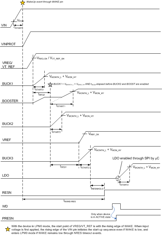
After the power-up sequence (described in Figure 8-4), all blocks are fully functional. BUCK1 starts first. After tSEQ2 elapses and BUCK1 is above the undervoltage threshold, BUCK2 and BOOST start. BUCK3 and VREF start one tSEQ1 after BUCK2. After the release of RESN pin, the µC can enable the LDO per SPI by setting bit 4 LDO_EN in PWR_CONFIG register to 1 (per default, this LDO_EN is set to 0 after each reset to the µC).
In case any of the conditions listed below happen during power-up sequencing, the device enters ERROR mode and the error counter (EC) is increased:
- Overtemperature on BUCK1-3 or VREG
- Overvoltage on BUCK1-3 or LDO
- Overcurrent on BUCK1
- SMPS clock fail
- VT_REF/VREG undervoltage
- Loss of GND
In case VT > VTTH-H, the device transitions to TESTSTART.
 Figure 8-4 Power-Up Sequencing
After the power-up sequence is completed (except LDO) without detecting an error condition, the device enters ACTIVE mode.