JAJSNJ1H May 2013 – December 2021 TPS65310A-Q1
PRODUCTION DATA
- 1 特長
- 2 アプリケーション
- 3 概要
- 4 Revision History
- 5 概要 (続き)
- 6 Pin Configuration and Functions
- 7 Specifications
-
8 Detailed Description
- 8.1 Overview
- 8.2 Functional Block Diagram
- 8.3 Feature Description
- 8.4
Device Functional Modes
- 8.4.1 RESET
- 8.4.2 Soft Start
- 8.4.3 INIT
- 8.4.4 TESTSTART
- 8.4.5 TESTSTOP
- 8.4.6 VTCHECK
- 8.4.7 RAMP
- 8.4.8 Power-Up Sequencing
- 8.4.9 Power-Down Sequencing
- 8.4.10 Active
- 8.4.11 ERROR
- 8.4.12 LOCKED
- 8.4.13 LPM0
- 8.4.14 Shutdown
- 8.4.15 Wake Pin
- 8.4.16 IRQ Pin
- 8.4.17 VBAT Undervoltage Warning
- 8.4.18 VIN Over Or Undervoltage Protection
- 8.4.19 External Protection
- 8.4.20 Overtemperature Detection And Shutdown
- 8.4.21 Independent Voltage Monitoring
- 8.4.22 GND Loss Detection
- 8.4.23 Reference Voltage
- 8.4.24 Shutdown Comparator
- 8.4.25 LED And High-Side Switch Control
- 8.4.26 Window Watchdog
- 8.4.27 Timeout In Start-Up Modes
- 8.5 Programming
- 8.6 Register Maps
-
9 Application and Implementation
- 9.1 Application Information
- 9.2
Typical Applications
- 9.2.1 Buck Controller 1
- 9.2.2 Synchronous Buck Converters BUCK2 and BUCK3
- 9.2.3 BOOST Converter
- 9.2.4 Linear Regulator
- 10Power Supply Recommendations
- 11Layout
- 12Device and Documentation Support
- 13Mechanical, Packaging, and Orderable Information
パッケージ・オプション
メカニカル・データ(パッケージ|ピン)
- RVJ|56
サーマルパッド・メカニカル・データ
- RVJ|56
発注情報
8.3.1.2 Normal Mode PWM Operation
The main buck controller operates using constant frequency peak current mode control. The output voltage is programmable with external resistors.
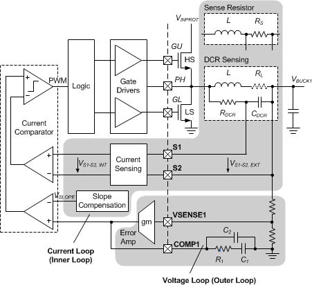
The switching frequency is set to a fixed value of ƒSWBUCK1. Peak current-mode control regulates the peak current through the inductor such that the output voltage VBUCK1 is maintained to its set value. Current mode control allows superior line-transient response. The error between the feedback voltage VSENSE1 and the internal reference produces an error signal at the output of the error amplifier (COMP1) which serves as target for the peak inductor current. At S1–S2, the current through the inductor is sensed as a differential voltage and compared with this target during each cycle. A fall or rise in load current produces a rise or fall in voltage at VSENSE1, which causes COMP1 to rise or fall respectively, thus increasing or decreasing the current through the inductor until the average current matches the load. In this way the output voltage VBUCK1 is maintained in regulation.
 Figure 8-2 Detailed Block Diagram Of Buck 1 Controller
The high-side N-channel MOSFET is turned on at the beginning of each clock cycle and kept on until the inductor current reaches its peak value as set by the voltage loop. Once the high external FET is turned OFF, and after a small delay (shoot-through delay), the lower N-channel MOSFET is turned on until the start of the next clock cycle. In dropout operation the high-side MOSFET stays on 100%. In every fourth period the duty cycle is limited to 95% in order to charge the bootstrap capacitor at BOOT1. This allows a maximum duty cycle of 98.75%.
The maximum value of COMP1 is clamped so that the maximum current through the inductor is limited to a specified value. The BUCK1 controller output voltage is monitored by a central independent voltage-monitoring circuit, which has an independent voltage-monitoring bandgap reference for safety reasons. In addition, BUCK1 is thermally protected with a dedicated temperature sensor.