JAJSEQ5A August 2017 – February 2018 UCC24612
PRODUCTION DATA.
- 1 特長
- 2 アプリケーション
- 3 概要
- 4 改訂履歴
- 5 Pin Configuration and Functions
- 6 Specifications
- 7 Detailed Description
- 8 Application and Implementation
- 9 Power Supply Recommendations
- 10PCB Layout
- 11デバイスおよびドキュメントのサポート
- 12メカニカル、パッケージ、および注文情報
7.3.2 Synchronous Rectifier Control
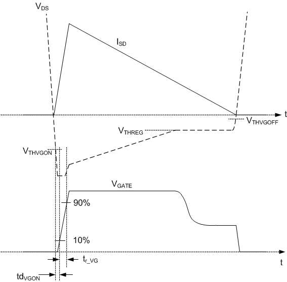
The UCC24612 SR controller determines the conduction time of the SR-MOSFET by comparing the drain-to-source voltage (Vds) of the MOSFET against a turn-on threshold and a turn-off threshold. The VG output is driven high when VDS of the MOSFET falls below VTHVGON and is driven low when VDS rises above VTHVGOFF as illustrated in Figure 17. Since when SR is conducting, its drain to source voltage (VDS) is negative, more negative voltage drop means higher SR current.
 Figure 17. VG Output With Respect to VDS
NOTE
Because of finite propagation delay and rise times, the body diode of the SR-MOSFET may conduct briefly after VTHVGON has been exceeded. A waveform similar to that depicted in Figure 17 can be observed during SR operation in a simple Flyback circuit.
It should be noted that before the SR turns on, there is a small delay caused by the internal comparator delay and the gate driver delay. During the delay time, the SR MOSFET body diode is conducting. For a Flyback converter, the SR current is at its maximum value during this delay time. It is desirable to have minimum delay. The gate driver design should avoid long turn-on delay.
For certain applications, this delay is essential for correct operation. In Active Clamp Flyback converters, especially when the primary-side switches are using Si-based super-junction MOSFETs, due to the large nonlinear junction capacitance, the SR often sees a leading spike current, followed by the real conduction current. Typically, a longer minimum on-time can override this spike to make the circuit operate normally. However, this forced minimum on-time can allow current that transfers the energy from output to input and reduces the overall converter efficiency. In UCC24612, two different versions are available. UCC24612-1 has an inherently short turn-on propagation delay (80 ns typical) and can be used with the converters that need shorter delay, such as standard Flyback converters or Active Clamp Flyback converters using GaN MOSFETs as main switches. UCC24612-2 has a longer 170-ns turn-on delay, to further ignore the leading edge spike and can be used with Active Clamp Flyback using Si-based super-junction MOSFETs as the main switch or LLC converters. Due to the longer turn-on delay, UCC24612-2 also increases its minimum on time-to 540ns to allow further enhancement on dealing with resonant-shape current, which makes a better choice for Si-based super-junction MOSFETs as the main switch or LLC converters.
When the SR body diode is conducting, the VD pin becomes negative with respect to the VS pin, by a body-diode drop. The connections of VD and VS pins should be tracked directly to the SR MOSFET pins, to avoid any overlap of sensing and power paths, minimizing the negative voltage and ringing caused by the parasitic inductances. Low package inductance MOSFETs are preferred to minimize this effect.
Besides the simple comparator, UCC24612 also includes a proportional gate driver for the SR. For conventional SR control, the SR MOSFET is always driven to the full driving voltage. This minimizes the conduction loss. However, this method has some major drawbacks. The turn-off threshold is often a fixed value, to prevent shoot-through, so that the SR is turned off before its current reaches zero. This causes SR body diode conduction and actually increases the conduction loss. Another issue is associated with operation in continuous conduction mode (CCM) condition. When a Flyback converter operates in CCM, the SR current slope (di/dt) at turn-off could be as high as 150 A/µs. This high current slope could cause large negative current due to long propagation delay. Furthermore, the delay caused by discharging the SR MOSFET gate from full voltage to its threshold level introduces another delay, further increasing the negative current.
Instead of keeping the SR MOSFET turned on with full gate driver voltage, UCC24612 reduces its gate driver voltage when the voltage drop across SR drain-to-source reaches -50 mV (current approaching zero). During this time, UCC24612 tries to regulate the SR voltage drop to -50 mV. This brings two major benefits to the application: a) Preventing the SR premature turn-off, avoiding extra loss associated with body diode conduction and reverse recovery, b) Shorter turn-off delay since the SR MOSFET gate voltage is already reduced close to the threshold level and the SR can be turned off with virtually no further delay. Since the -150 mV is the maximum level that can be achieved by the UCC24612, the SR MOSFET selection should allow the -150-mV threshold to be activated when operating in deep CCM condition.
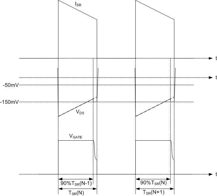
In certain applications, such as telecom DC/DC bricks, due to the lower input and output voltages, operation in deep CCM mode (low inductor current ripple) gives the benefit of less conduction loss. In these applications, the SR turn-off current is high and the SR MOSFET voltage drop can still be less than the -50-mV threshold. UCC24612 decreases the -50-mV threshold to -150 mV to force proportional drive activation and reduction of the gate driver voltage for a fast turn-off. The timing to decrease the threshold is based on previous cycle SR conduction time. Because the regular proportional gate drive and the turn-off mechanism are kept functional continuously, the UCC24612 can still provide correct SR control even for a large SR conduction time change within two switching cycles. The forced proportional gate drive mechanism can be shown in Figure 18. In Figure 18, the turn on delay was ignored to simplify the illustration.
 Figure 18. Forced Proportional Gate-Drive for Deep CCM Operation
For Flyback converters, the SR current starts from its maximum amplitude and keeps reducing. Proportional gate drive is only enabled at the later part of the SR current conduction period. However, for other topologies such as LLC or Active Clamp Flyback, the SR current starts from lower amplitude and then increases to a higher amplitude. To prevent the proportional gate drive from being enabled at the beginning of the conduction period, proportional drive is disabled for the first 50% of the SR conduction time, based on the previous cycle SR conduction time. In this way, the proportional drive is always enabled on the current falling slope and minimizes impact on the conduction loss.